

 |
HP 35 hardware in depth analysis. In the following pages, I present an exhaustive
analysis of the HP35 hardware. As of Sept 2009, I have completed the hardware
analysis.
This study was started during the months
of April 2006 on a bunch of fully working HP35, (starting with SN 1212313213 type 2,
) with a few multimeters, LCR bridge (Capacitance, Resistance & Inductance tester),
Transistor tester, and my old oscilloscope
HITACHI (model 422 40 Mhz, double trace).
It has been
constantly updated and augmented since.
Many calculators HP-45, 55, 65, 21, 25 and 67 were analyzed at the same level of
accuracy to understand differences in the hardware.
I hope I'll have the courage to publish all
this material.
|
 The reader can recognize on this photo the components of the dismantled
HP 35 calculator,
split into two PCB, connected by 25 pins and powered by a genuine HP power pack.
That was the very start of the story.
I reconstructed on 'breadboard machines' -with modern components- many basic
hardware parts (power supply unit, Led display etc).
I swapped parts between different models (HP-35, HP-45, HP-55).
I used Spice to simulate dynamically bipolar sections
(Power Supply Unit, Clock Driver).
I constructed a ROM reader to validate object code (buggy
HP-35).
Finally I traced every signal on the 2 PCB (clocks, addresses
and instruction data ...), so even if it may remains errors, I believe
honestly it is a fairly good
description of the calculator electronics - statically and dynamically.
1) The small PCB 1 can be divided in 6 parts:
a- left, the white chip is the Control and Timing
circuit(1820-0849),
b- center, the 3 ROMS in their 10 pin TO99 metal cans,
c- right, the 2 chips are - with a golden top- the Arithmetic and Register
circuit (1820-0848),
d- and above it the clock
driver,
e- Top right, on the PCB 1, 2 transistors and 7
passive components form the "one shot" Schmidt trigger used to deliver a PWO
(power on) signal to the rest of the machine,
f- Top left, 2 transistors, a pulse
transformer and 15 passive components form the DC to DC converter (PSU - Power
supply unit), that creates from a single 3.75 V DC the three supply voltages of
the machine:
Vcc = +7.5 V,
Vss = 6 V,
Vgg = -12 V.
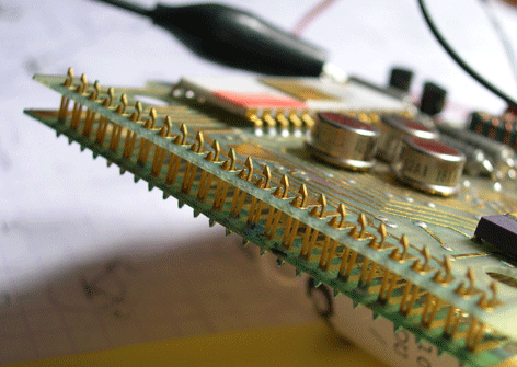
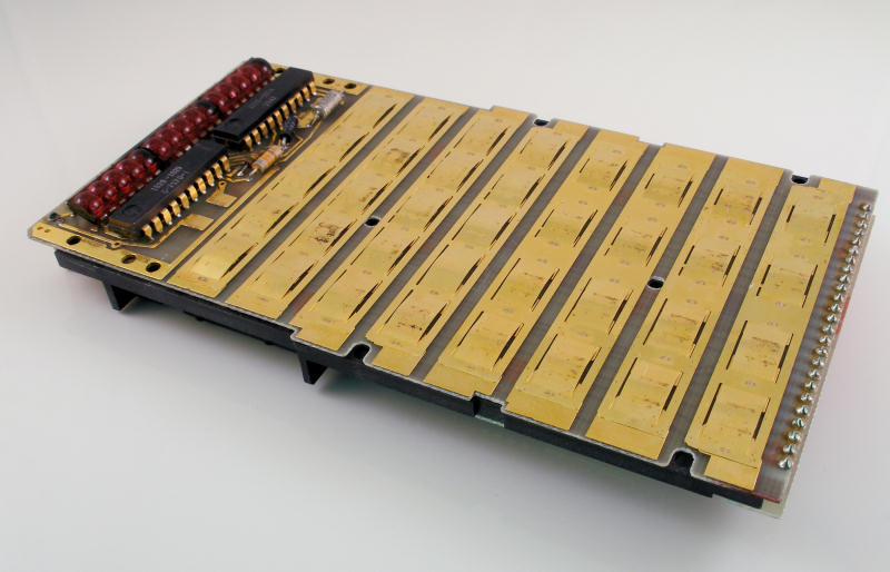
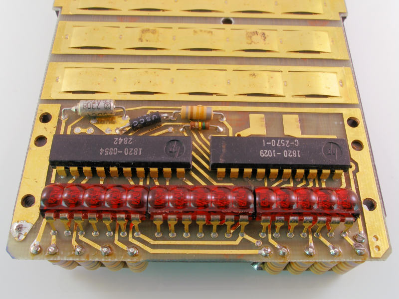
2) The bigger PCB 2 -that is linked to the first by a
25 pin connector - can be divided only in 4 parts:
- the keyboard (golden "cricket" principle 35 keys),
- the 15 LEDs (in red) and
the 2 chips, respectively Anode driver (below) and Cathode driver (above)
and a few passive components resistors, LC circuit etc...).

The unit is powered by a battery pack (3 rechargeable
NiCad units of 1.25 V each - total V+ = 3.75 V) or by a power unit delivering a regulated and
limited current to power the calculator and charge the NiCad unit.
I will structure this my study as follows:
The chapter "Hardware basic design" will put the pieces together, showing the function of each
module and bus line, and will also discuss the system timing and the
synchronization issue,
Then (as sub chapters), I will cover in detail, the main 5 MOS/LSI
chips:
- "The Control and Timing circuit",
- "Arithmetic and Register circuit",
- "The 3 ROMs"
- the Clock
Driver,
- the Power on unit,
- the Anode driver,
- the Cathode driver,
- the Keyboard,
- the 3 inductor driven 5 LED clusters.
- the Power unit.

To establish a comparison, the same review as been conducted at the same time on
a HP25 (Woodstock) unit.
J. Laporte
May 05 2006, May 28 2007, revisited Sept 2009.
(Photos Daniel WEED, J. LAPORTE)
 The reader can recognize on this photo the components of the dismantled
HP 35 calculator,
split into two PCB, connected by 25 pins and powered by a genuine HP power pack.
 can be divided only in 4 parts: