A power-on reset circuit generates a reset signal when power is applied, ensuring so that a system starts operating in a known state.
The HP-35 uses a simple PWO circuit composed of a one-shot circuit (Schmitt trigger).
When the power supply is switched on, Vss (6v) provides
a small positive voltage on the base of Q2 (forward bias),
hence Q2 starts conducting. INIT is low.

The current thru R3 rises the voltage threshold for Q1
to turn on (upper trigger level) and, at the same time, R2 charges C1 and soon
the threshold is reached. Q1 switches ON and pumps the Q2 base current that goes
OFF consequently.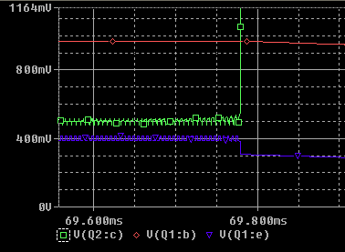
(On the probe screen
left : Q2's collector goes high,
when the difference between Q1's base and Q1's emitter is around 600mV.)
INIT is now high (@ Vss = 6V, logic 0) and
holds it there.
The circuit keeps the INIT signal at 0 volts for
about 70ms.
The Schmitt triger is driven by the R2C1 time constant and Q1 base is the input,
Q2 collector the output.
(many thanks to Bernhard to show me I was wrong incorporating the couple R4-D1
in the one-shot logic : it is -in fact - part of the MOS clock driver.)
This long delay (compared to the time word of the machine
= 280 us) gives
time to each of the 3 ROMS to be synchronized to the main system counter
(SYNC is high during bit time window b45-b54).
At its end, the state of the system is stable and INIT is at logic level 0 (+6v Vss), ROM 0 is active, ROM1 and ROM 2 are inactive, and the starting address “00000” is gated on line Ia (see below the schematics and 2 photos of the circuit on the main HP-35's PCB.
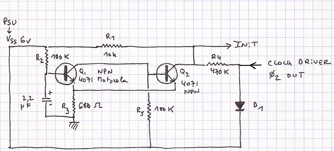
fig 1, power on schematic (J. Laporte 2007)
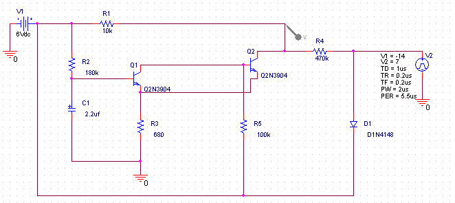
fig 2, "power on" Pspice's schematic (J. Laporte 2008)
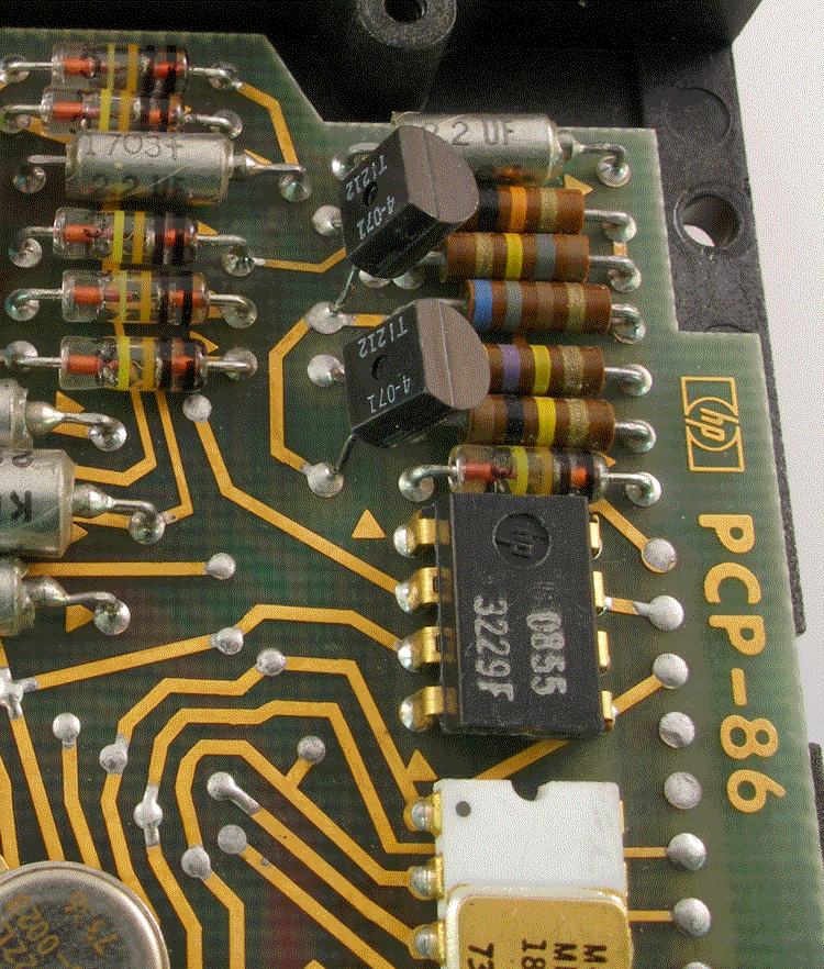
fig 3, power on circuit (photo D. Weed, 2007)
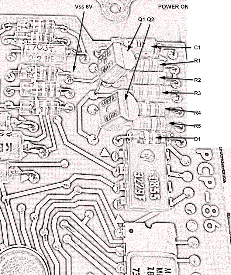
fig 4, power on commented schematic (J. laporte)