and other vintage HP calculators.
by Jacques LAPORTE and Daniel WEED
![]()
![]() The HP-35's POWER UNIT
The HP-35's POWER UNIT
and other vintage HP
calculators.
by Jacques LAPORTE and Daniel WEED
The early HP hand held calculators used dynamic MOS LSI circuits and therefore they needed a low power (≃ 100mW) power unit, providing 3 dc voltages:
- Vcc
8.2 V [for the cathode LED driver],
- Vss 6 V [for the clock driver, the control & timing, the ROMs and the arithmetic registers],
- Vgg -12 V [for the clock driver, the control & timing, the ROMs and the
arithmetic registers].
A
small switching power supply circuit was used to build those voltages from a
battery source or external DC supply :
- Vbsw 3.75V [3 * 1.25 V Nicad for the Classic series],
- Vbsw 2.5 V [2 * 1.25 V Nicad for the Woodstock series],
or from a wall plug-in adapter providing Vbsw = 3.6 to 4.7 VDC for the Classic
series.
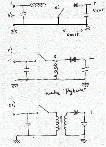
The scheme used is rather classical : a step-up « boost » converter is used to build Vcc and Vss (Vout > Vin) while an « flyback « converter configuration is used for Vgg (-12V).
The electric model for both DC-to-DC configurations can be found in all good text books (see for example Horowitz and Hill, 2nd edition p. 358) ; sketches 1, 2 and 3 illustrate the concepts.
Since the inductor is either off or saturated, this approach is very efficient and there is little dissipation.
Let us
say a few words about it.
When the switch is closed (scheme 1), the current is flowing into the inductor
which is where the energy is stored.
When the switch is open, voltage at point X (diode's anode) rises since the inductor tries to maintain a constant current; when the diode is passing, the current is flowing into the capacitor through the diode (Vout > Vin).
In the flyback configuration (scheme 2), the inductor pulls voltage - at point X (diode's cathode) - negative in order to maintain the current flow, and the current is going into the inductor from the capacitor (output is negative).
In the third configuration (scheme 3) a transformer is used to couple the switcher to the rest of the circuit allowing a fine tune of the output voltage.
1)
The DC-DC converter.
The switching device today could be a low-power IC. But at that time (early 70s) the designers had to build the DC-to-DC
converter with discrete components.
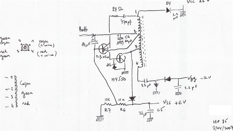
The switching element in the HP-35 uses two complimentary transistors (PNP and NPN) and a small transformer, forming a blocking oscillator.
Figure 5 below shows the diagram of the HP-35 PSU.
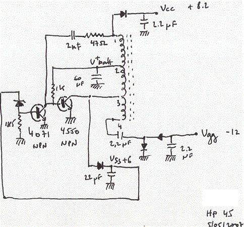
The PSU evolved slightly for the HP-45 (Figure 6) and for the Woodstock series (Figure 7 & 10) : 2 NPN transistors were used instead of the complementary NPN-PNP pair.
In each case, the battery or wall plug-in voltage (Vbsw) is applied at point 2. The oscillations are transformed at point 1 through a diode and smoothed by a capacitor to a Vcc of +8.2 V, and in opposition at point 4 through a pair of diodes and a capacitor to produce Vgg -12V.
Fig 4
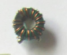 The transformer has one
long winding around a torroidal core. The winding is made of three wires each
with a different number of coils, resulting in four points as labeled in the
schematic. The wires are red between points 3 and 4, copper color between
points1 and 2, and green between points 2 and 3. This transformer is shown in
Figure 4.
At point 3 (green winding) -through a diode – the Vss +6V is available.
Note the similarity in the case of the HP-45 (Figure 6) and HP-25 (Fig. 10) : only the design of the oscillator is changed.
The HP-35 power supply (Fig. 5)
See
below diagram and photo of the HP45's PSU
The HP-45 power supply (Fig. 6)
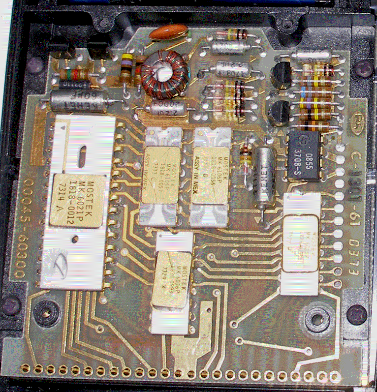
This pattern is used in all Classics and Woodstocks (see fig 7-1 the HP-67 diagram & 7-2 the HP-97's).
On the HP-67 diagram, the transistor Q2 and the toroidal transformer form the basic inverter.
Winding
1-2, Q2 and the RC cell (3900 pf, 150Ω)
oscillates at around 200 khz. From winding 2-3 Vss (6.25V) is derived, rectified
through a diode and filtered by the 22uf cap.
Vgg
(-12V) is derived from winding 3-4 as usual.
Vss is regulated by controlling the frequency of Q2 through the action of the zener
diode biasing Q3.
Fig 7 -1 : HP-67 power unit.

Fig 7 -2 : HP-97 power unit (after HP-97 service manual).

(same diagram as for the 67, but drawing of winding B and C are inverted)
See my HP 67-HP 97 Spice simulation.
2) The wall plug-in power supply.
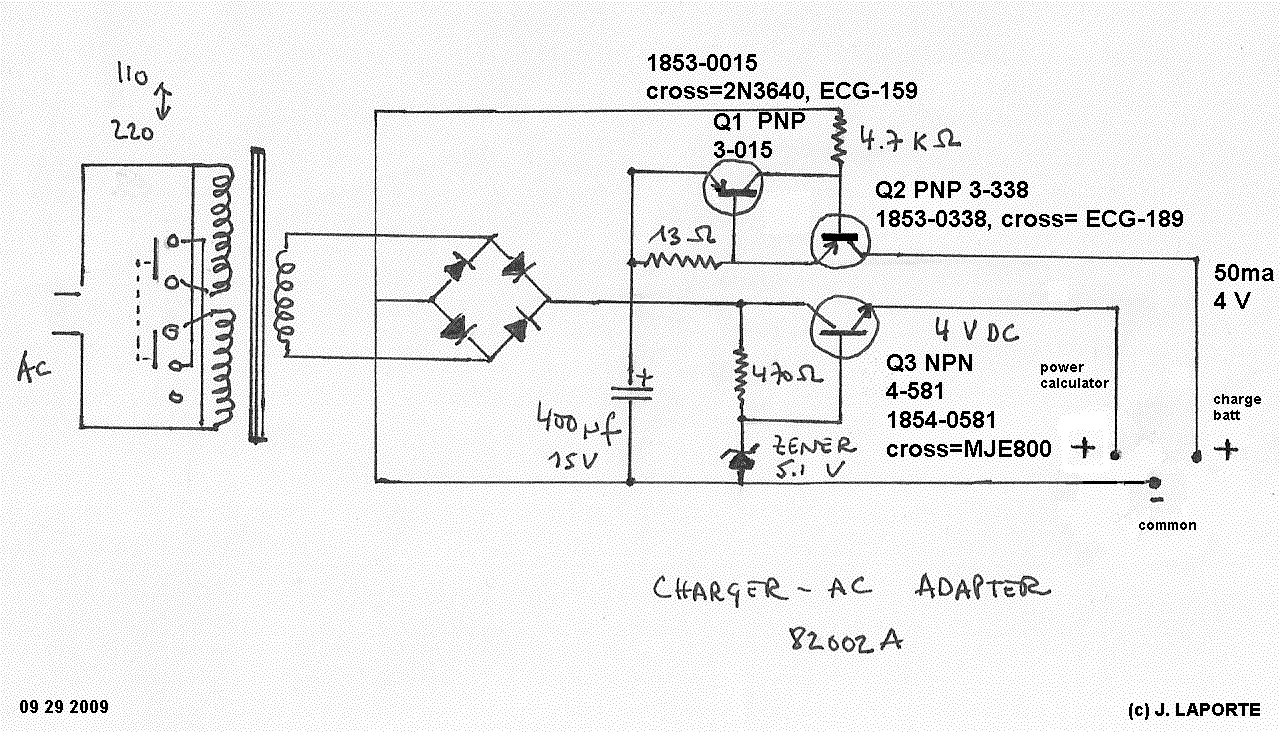
The Classic series (HP-35, HP-45, HP-55, HP70, HP-80 and HP-65) wall transformer power unit (Figure 7) is simple and robust, providing a constant voltage for the logic supply, and a constant current for charging the batteries.
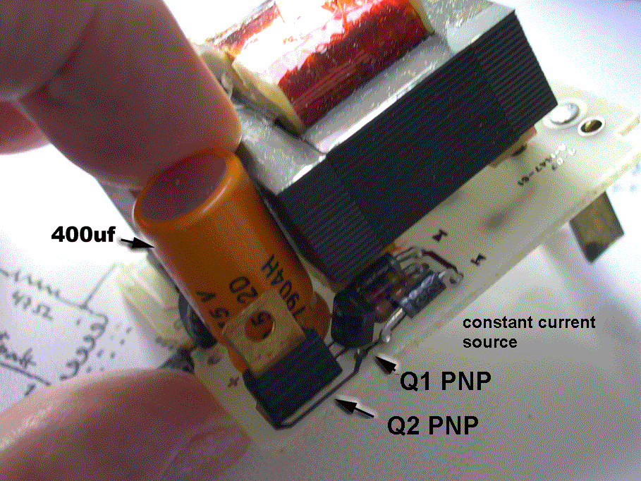
The transformer provides about 16 volts output which is converted to DC by a diode bridge and smoothed by a 400 MFD 15V capacitor. The resulting 15 Volt output feeds the logic supply and charging circuit.
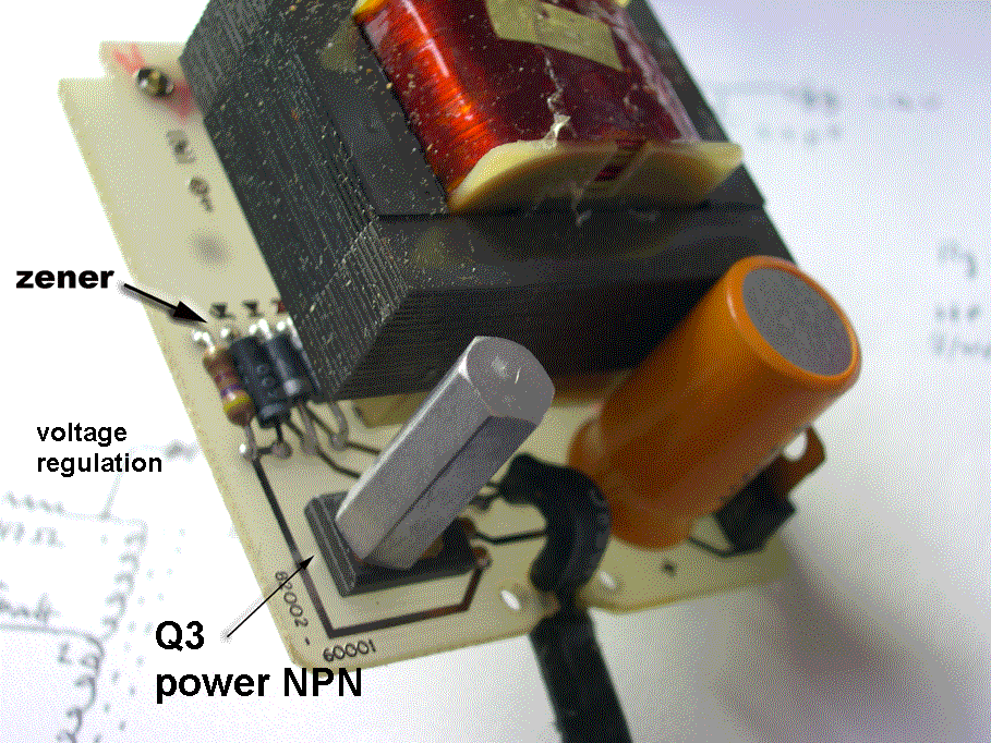
The logic supply voltage is regulated by a simple emmitter-follower circuit using a 4.7V Zener diode and a heat sinked power transistor. The 0.6V drop across the Collector-Emitter results in an output voltage of about 4.2 Volts. The charging circuit provides a constant current of 50-60 mA using 2 transistors (PNP and NPN) .
The same scheme is used in the case of the HP-67 also even though the HP-67 logic circuits are based on the second generation design.
The HP-97 however is quite different: the wall adapter outputs 8 VAC, not DC, the conversion to DC is done internally and (fig7-2) a 2 transistor over voltage circuit (Q4-Q5) is preventing Vb (battery) from rising above Vss (6.25 Vdc).
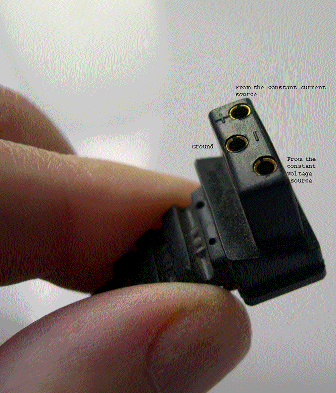
Below in Figure 8 is the schematics and photos for the wall plug-in supply type 82002A for Classic series (HP35, 45, 55, 65 67, 70, 80).
The wall plug-in supply is connected to the machine with a 3 prong plug :
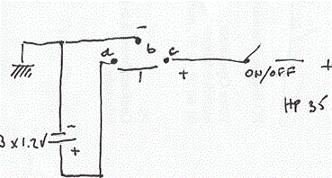
When the machine is powered by the battery a spring short-circuits point a and c (see Figure 9 sketch and photo below).
Fig
9
For its next generation (HP-21, HP-25 etc), HP adopted a cheaper approach much like the HP-97. There is no current limitation and no voltage regulator in the wall plug-in that is - in fact - just a transformer in a box (mains to 10 V AC) (see fig. 10).
Note that in this case (HP-25 and HP-21) the charging current is limited (135 mA) by a single resistor 8.2Ω in series with the Nicad's internal impedance (around 0.2Ω).
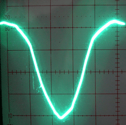
The two Nicads are forming a diode clamper circuit, for the half-wave rectifier (secondary voltage is 10V AC RMS and at point A9 on fig. 10 the DC voltage is around 4.1V).
It's an average since it's not a steady dc but a pulsating dc wave (positive half-cycles).
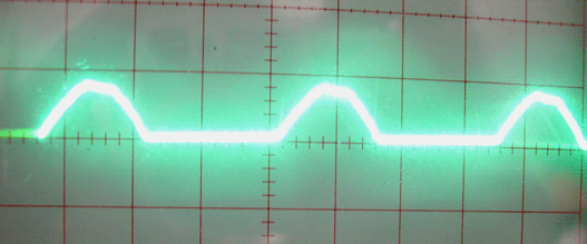
The voltage at point A2 on fig. 10 is around 2.9 VDC, if the Nicads are correctly connected. If not (frequently the case of old machines) the voltage can spike up to 10 Volts causing the destruction of internal MOS circuits, in most cases the RAMs.
HP-25 (HP-21) power supply (Fig 10) (pins A1 to A9 and B1 to B9 are connecting the logic board to the keyboard) :
 See note (1)

HP25 Main PCB board
details of the power supply unit, can be seen, at right:
- transformer,
- npn 2-transistor switcher,
- current limiter resistor,
- simple rectifier.
The
photo below shows an HP-25 on the bench connected to the AC adapter but
without Nicad in place.
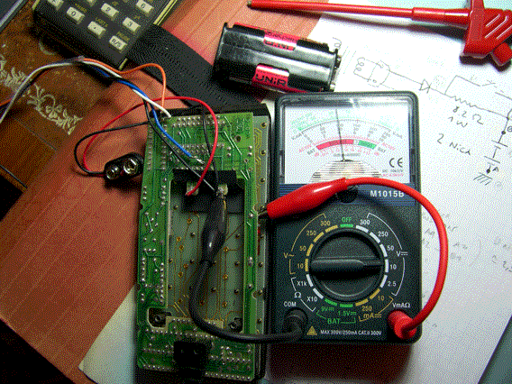 With
Nicads in place the current through the batteries is:
without adapter - 130 mA to point A2 (discharge),
with adapter:
slide off, 130 mA from adapter,
slide on, 100mA from adapter,
Without Nicads
Slide off: the voltage at point A2 is around 2.90 VDC : safe.
Slide on: the voltage rises up to 10 V.
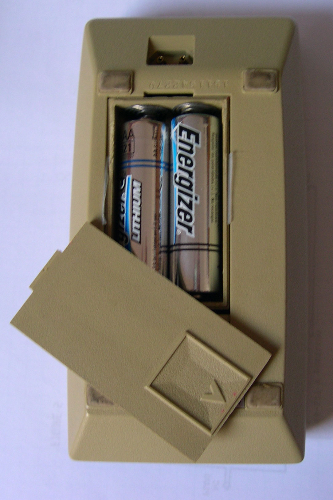
Warning: Good contacts between the batteries and the calculator are
mandatory and alas there is no much room inside the box to install a serious
voltage regulator.
My best advice is to use Nimh cells (charged outside) or -as I do- lithium
batteries (even if they put 1.5 per cell).
And forget about the HP charger.
(photo JL 2008-2009)
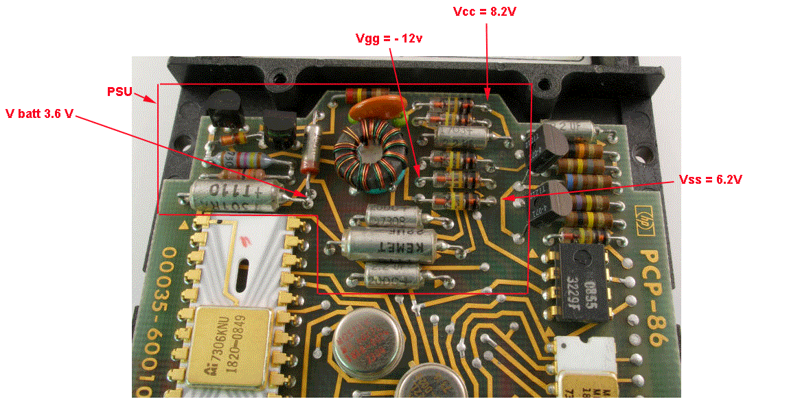
HP35 Power
Supply details (© photo Dan. Weed - 2007,
comments J.Laporte)
More details here
HP35 battery craddle and wall plug-in (© photo Dan. Weed - 2007)
H55
logic pcb
with the same PSU as the 45 (transistors are NPN 4 094 (equivalent to MPS3646) and
NPN 4 550)
On this photo, the
1N34 Ge diodes
can be identified easily using their Jedec colour code.
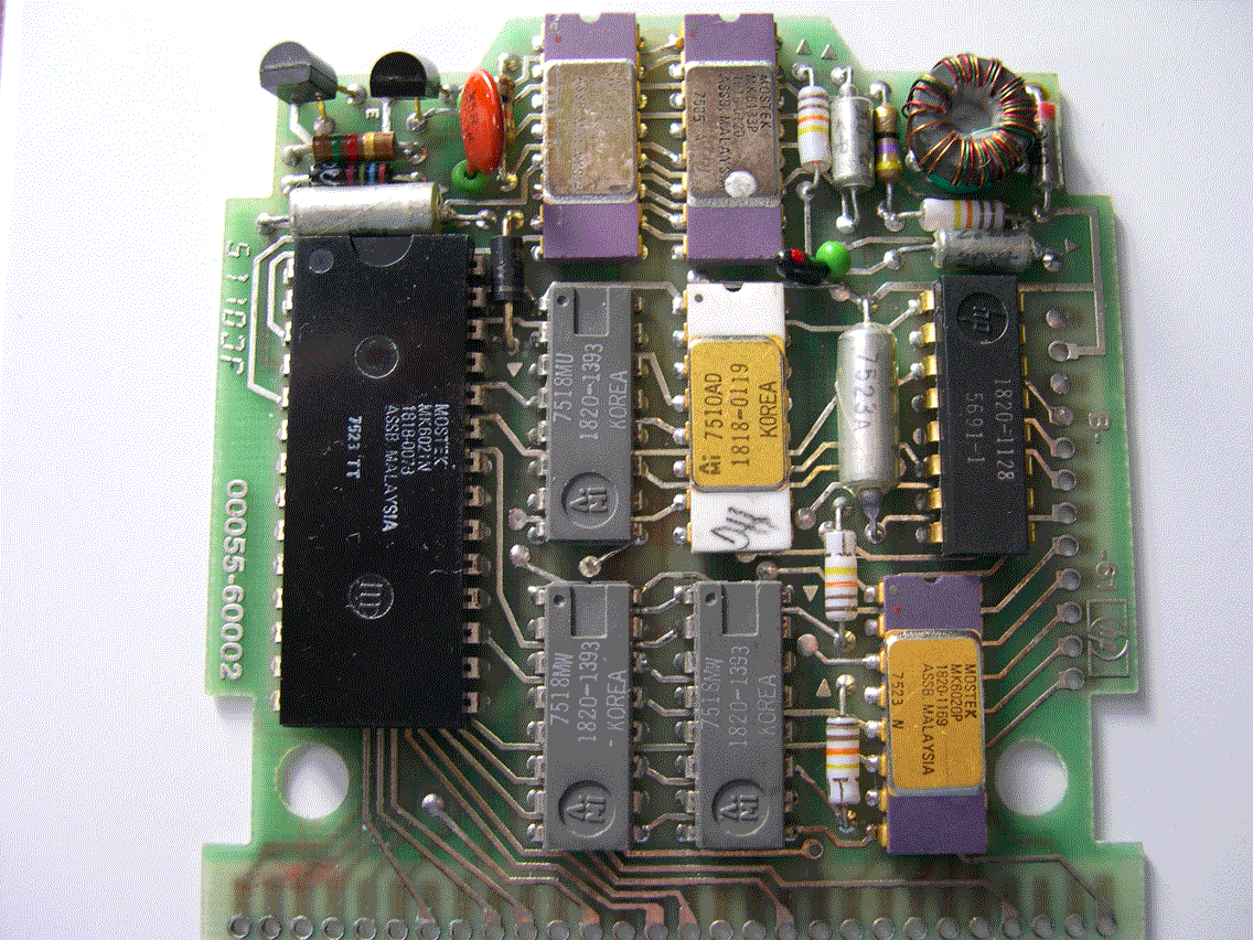
The
HP-65 PSU is very much alike. The 45, 55 and 65 use the same pair of transistors
:
- switcher 4-550 (HP part 1854-0550),
- regulation 4-094 (1854-0094)
The HP part 1854-0094 is listed in the HP replacement part cross ref :
equivalence PN 3646.
The 4-550 replacement is the 2N3904.
The close up pic below has been provided kindly by
John Robinson.
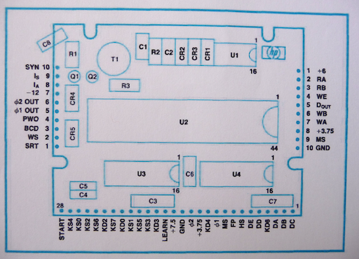
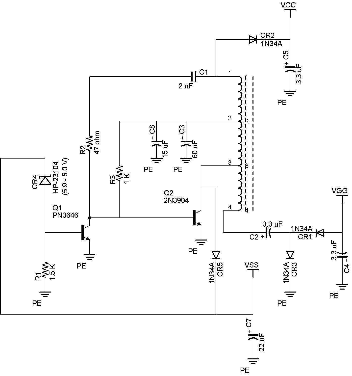
The PSU components can be clearly identified. The pic is followed by a layout
schematic of the 65 board (from the HP Journal may 74), with the same
orientation. John has drawn the 65 DC-DC converted schematic using a CAD package
(Eagle PCB). Obvioulsly, the component names are the same used by HP in the
layout schematic.
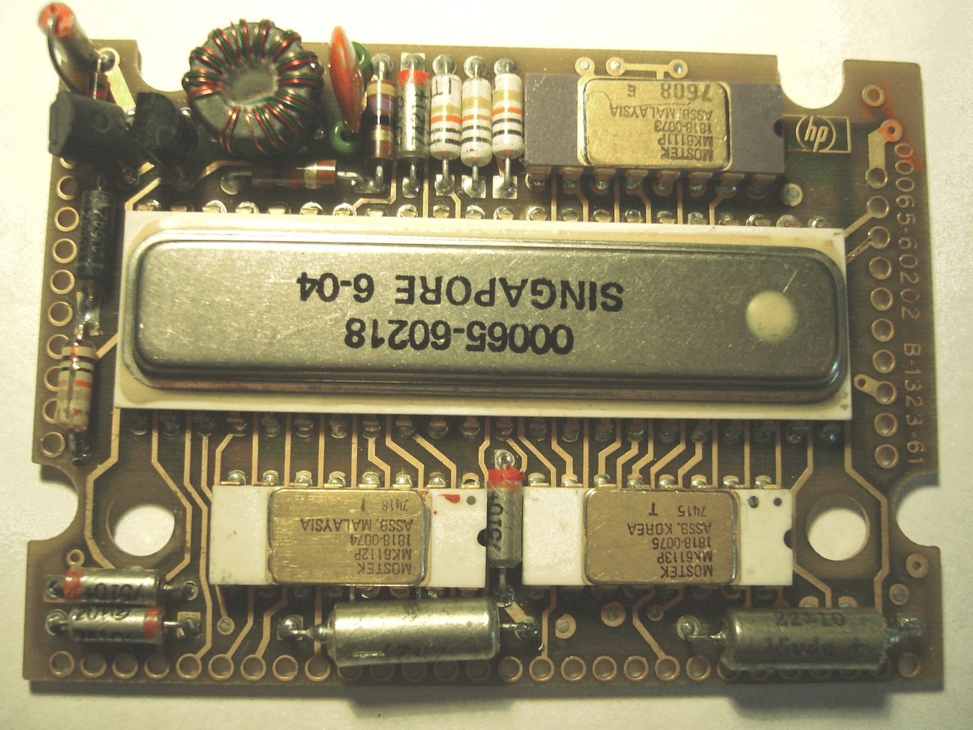
© photo J. Robinson - 2009
May
28 2007
revisited 11/2008, 10/2009, Sept 2010.
(1) I recently corrected an error, in my schematic of the HP-25 DCDC converter, sorry.
The Woodstock's display used a different principle than the Classic's ; the display driver circuits do not use a Vcc voltage @ 7.2V (higher than Vss) but a lower voltage at around 4.4V.
I named it Vdisp to avoid confusion.
So only 3 voltages are built by the Woodstock converter : Vss @ around 6V, Vgg @ around -12V and Vdisp @ around 4V (HP-67 and HP97 are special cases :
only 2 voltages are built by the DCDC converter).
My old friend Pspice, when solicited this summer for the Woodstock study (coming out soon) demonstrated clearly and forecasted brilliantly that the voltage at the anode of diode D4 must be somewhat around 4.4 DC (lower than Vss).
I checked carefully the circuit and voltages on real machines HP-21, HP-25 and HP-25C.