![]() A
HP power unit Spice model (all the LED calculators Classic, Woodstock ….)
A
HP power unit Spice model (all the LED calculators Classic, Woodstock ….)
by Jacques LAPORTE.
1) Taking a HP calculator power unit into pieces.
The HP « hand held » calculators are operated with 2 or 3 Nickel-Cadmium AA batteries. Their semiconductor P-MOS technology requires 2 or 3 reference voltages : Vcc = 7Vdc, Vss = 6 Vdc and Vgg = -12 Vdc.
A circuit named power supply unit (PSU) is building these voltages from the battery 3 * 1.2 = 3.6V or 2 * 1.2 = 2.4V.
The type of circuit used is a simple switching supply (boost since Vout> Vin) and flyback (Vbatt ->Vgg = -12V
In most cases (HP45 => HP97) a single
transistor forms an oscillating circuit and its output is rectified and
filtered to derives Vss.
This main positive voltage Vss is also regulated by another transistor (its base
beeing biased by a follower and a Zener diode).
The output is then doubled and inverted to produce Vgg @ -12V.
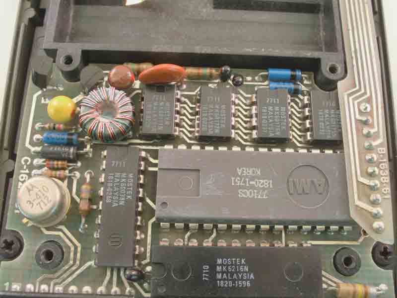 HP 67 PSU (photo D. Weed)
In the
case of the HP-67 power unit, there are 15 components:
- 1 tri-windings toroidal transformer,
- 2 NPN transistors,
- 3 rectifier diodes,
- 1 Zener diode,
- 3 resistors,
- 5 caps (4 electrolytics).
2) The toroidal transformer
The little transformer can be seen on the main PCB (below) of each model of HP LED calculator.
Its function is to form with a NPN transistor a small blocking oscillator.
The inductances are not documented.
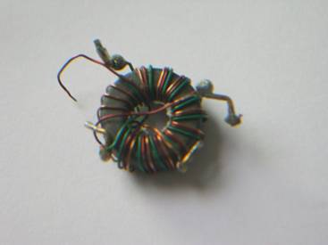
Unwinding the 3 copper wires, I noticed the trifilar winding was made of copper
insulated with an enamel coating.
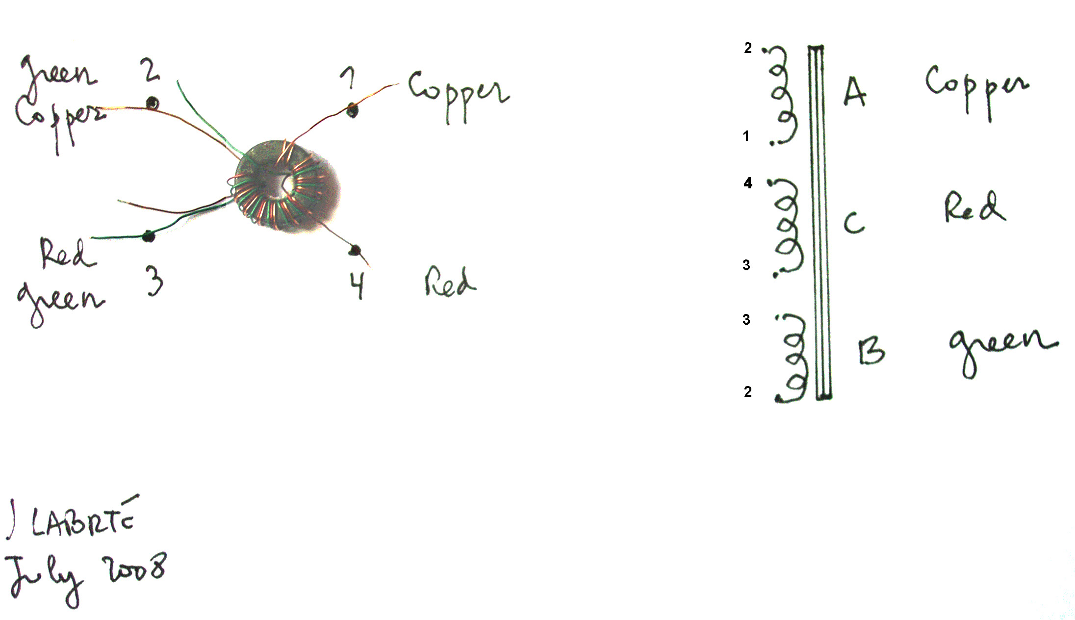
The three windings are colored (copper, red, green) and the toroidal transformer is mounted on a blue plastic pad soldered on the PCB by 4 pins numbered after HP-97 service manual (photo 2):
1-2
winding A, copper wire, LC cell,
3-4 winding C, red wire, (inverter)
2-3 winding B, green wire, primary (Q2 collector).
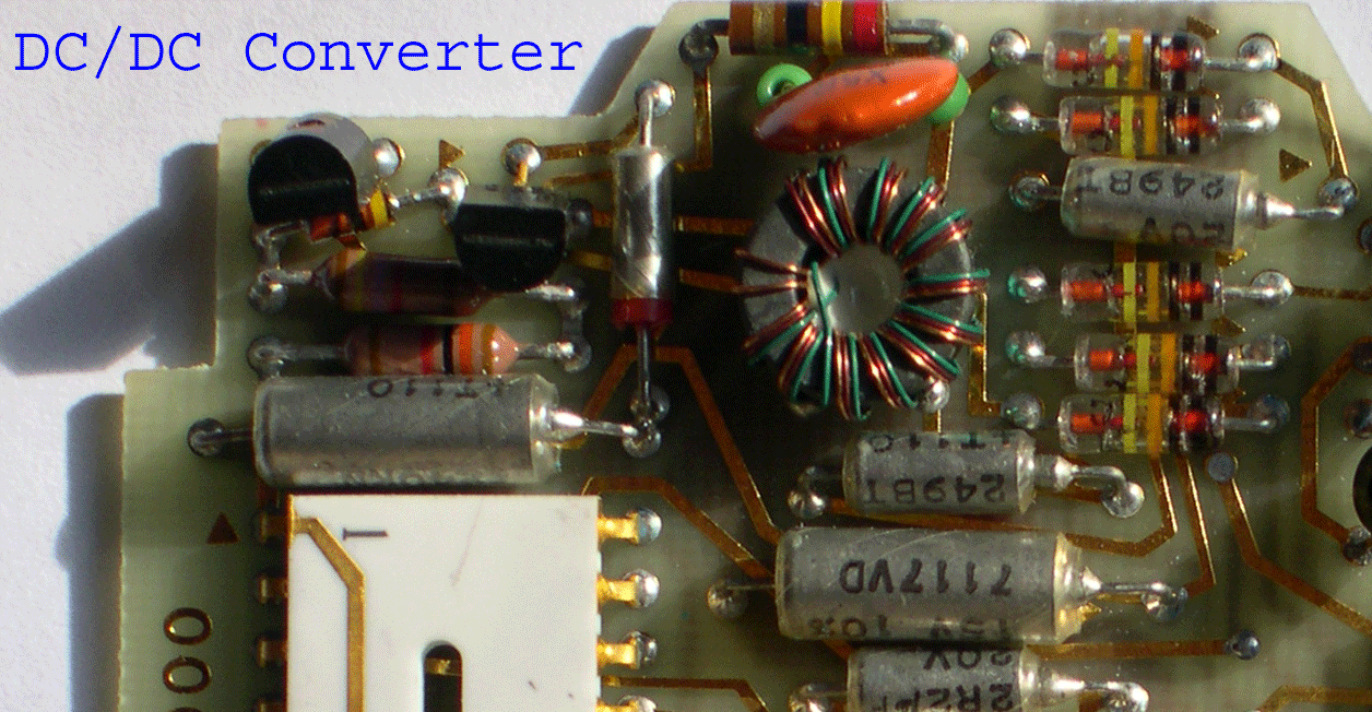
The winding is realized in a trifilar way (each colour side by side and "in phase") around a toroidal (ring-shaped) iron powder core.
The toroidal radius is 0.4 cm and the core radius is 0.2 cm, that gives a cross section area at A= 0.125 cm2.
A HP-35 PSU
There are 12 turns of green and red wire and 15 turns of copper wire.
Relative
permeability of the core is unknown but can be calculated as k=1100.
Direct measures of inductances (with a Voltcraft LCR-9063 bridge) give : Inductor B and C around 110 uH and inductor A around 150-190 uH (on a HP35).
3)
Active components
On the 67-97:
The Zener diode is of unknown type but has a zener voltage at around 6Vdc
On the 35, 45, 55, 65:
Diodes are
Ge types (1N34) ; their forward voltage drop is low probably
around 0.3V .
A modern equivalence could be type 1N60 or 1N270.
(Toroidal transformer)
The two transistors are generally NPN labeled Motorola 4-094 and 4-550 ; except for the HP-35 which has a NPN-PNP pair for the switcher : HP part 1853-0020 a "special pnp" also labeled 3-020 on some schematics and 1854-0550 a npn also known as 4-550.
The
NPN 4-550 has been replaced with success with the genuine 2N3904
to repair PSU of HP45, HP65 and HP67. It must be very close. The equivalent for
NPN 4-094 HP part 1854-0094 is the PN3646 (Fairchild).
4) The HP67-97 Spice deck
This study is valid for all the LED calculators (HP 45, 55, 65, 67, 97 etc...) using a 2 NPN circuit.
I started from the schematic published by HP
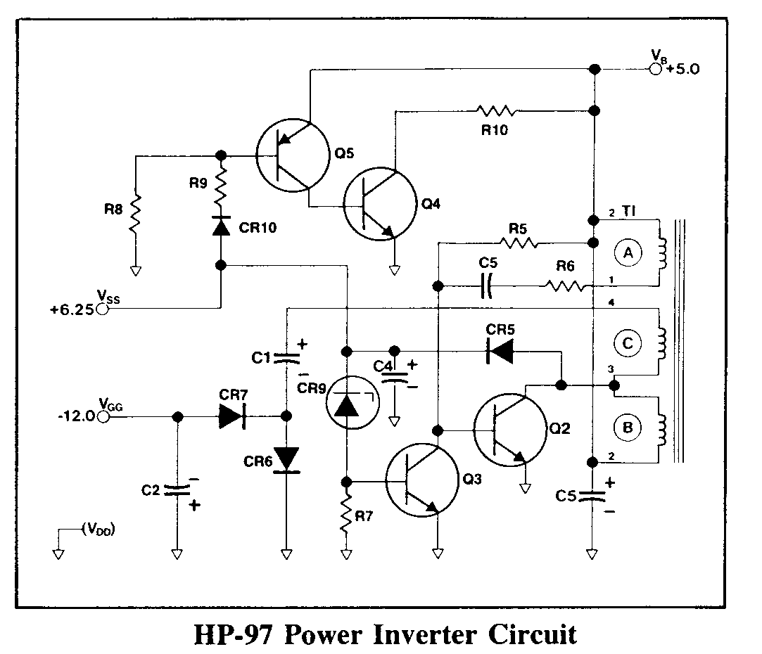
The
first Spice model (below) shows the blocking oscillator alone.
It is based on a NPN transistor whose output is coupled to the input through windings B (the transformer 'primary') and A of the pulse transformer.
The winding polarities are so chosen to provide a regenerative feedback (dot convention : a dot must be placed on each winding end marked #1 by 'OrCAD's Capture').
When the power is supplied, the capacitor C5 (3900 pf) is charged due to the current through resistor R5 and R6. When its 'cut in' voltage is reached, the NPN transistor goes into conduction and the blocking oscillator cycle begins.
The collector current flows through winding B and a positive feedback (emf) is induced to winding A and charges further C5, the EB junction being more and more forward biased.
When the BJT reaches saturation, no further increase in collector current is possible. The rate of change of flux in winding B is zero, no more induced voltage in winding A and the base current drops to cut off.
The NPN remains at cut off as the charge of the capacitor leaks away and when the reverse bias on the NPN is removed the cycle restarts.
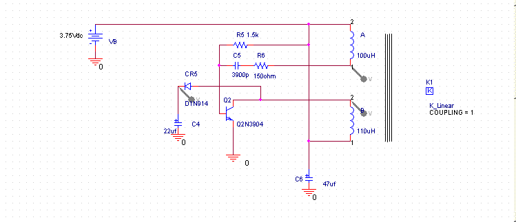
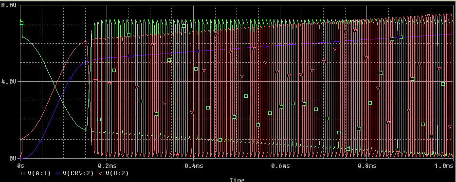
Vss (6Vdc) is derived from winding B, rectified by diode CR5, filtered by C4 (22uf).
The Pspice simulation demonstrates the switching pulse and the Vss at 6vdc.
The next
schematic adds
- Vss regulation Q3 and Zener,
- the inverter deriving a negative voltage from winding C,
rectified by CR6, CR7, filtered and doubled by C1 (2.2uf) and C2 (2.2uf).
The blocking point is regulated by controlling the bias of Q2 through the
action of a current source Q3 with a Zener between Vss and its base (when Vss is under the Zener voltage (Vz) Q3 is cut off and Q2 is saturated, when Vss is greater than Vz, Q3 is saturated and Q2 is cut off).
The doubler circuit for Vgg is classical. During the positive half cycle of winding C's voltage D6 conducts but not D7 and charges C1 to peak voltage with inverted polarity (-Vss).
During the negative half cycle D7 conducts but not D6 charging C2 to -Vss.
At this moment of the cycle the voltage across cap C1 is in series with the input voltage : the total volatge is 2 * (-Vss) = -12V (Vgg).
Next on the positive half cycle, the diode D7 is blocked and the capacitor C2 discharges through the load.

The next probe screen capture -after Pspice simulation- shows the switching pulse and the two voltages derived Vss @ 6Vdc (yellow) and Vgg @ -12 (purple line). Neat.
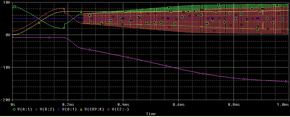
This spice model has been realized with HP-67 & 97 units ; but it is valid for the Woodstocks HP21 HP25 .... and for the HP-45, HP-55, HP-65 etc ... in fact for all the HP models with a 2 NPN power units.
It is
easy to have an 2N3904 or equivalent starting to pulse with the right bias on
the base and the right charging current for the capacitor : 1.5k to Vbatt on the 67, 1k on the 45 or 680ohms on the HP-25.
This 2 NPN arrangement was started with the HP-45 (the oscillating NPN is
labelled 4-550 and the regulating NPN is named 4-094) and was kept in the future.
5) The HP35 Spice deck
Earlier for the HP-35, HP used a more delicate scheme : the oscillation is
driven by a PNP-NPN pair reaction that makes the circuit component dependent : the 2
transistors must match perfectly. The circuit is overall quite comparable it is basically a blocking oscillator using the early 70's state of the art. The switching device is a NPN transistor but the constant current source is a PNP partner.
These old transistors are really difficult to
find, no specs are available, making HP-35's PSU difficult to analyse and
repair.
As a
matter of fact, I had to repair (August 2008) two of my HP-35 "breadboard"
units.
Symptoms: No Vcc, Vss, or Vgg... but Vbatt. Bad day but a chance to test
my own medecine !
a) On the first unit, I checked the two transistors and found that the 4-550 (switcher) was burnt. I checked
every diode on the PCB and found 3 diodes dead.
The
NPN in the 35 is named 4-550 (HP part 1854 0550) and the PNP is 3-020 (HP part
1853 0020) ; they have high beta.
1853-0020 happens to be a PNP Silicon Military Transistor manufactured (in the
70's) by MOTOROLA, Mfg. Part #5961-00-904-2540.
The 3-020 is mentioned in the the "Barney Oliver
Audio Amplifier" schematics (thanks to
Kenneth Kuhn) and as we will see in the Spectrum Analyser 8556A maintenance
manual.
I replaced the 4-550 with a genuine 2N3904 out of the box, the diodes
(1N34 Ge 0.270V forward drop) from another dead unit, but I could have taken
modern 1N270. The unit is now working well.
That confirmed the equivalence between 4-550 and 2N3904.
b) On the second unit, the 2 transistors were dead and I had to replace them
(August 17 2008) by
modern equivalents : 2N3904 and 2N3702: see the full story note
(2).
Searching deep into my HP documentation, I found out
the equivalence of the second BJT (PNP) ; in the SPECTRUM ANALYZER Hewlett-Packard model 8556A
(low-frequency) Maintenance Manual (Including repair parts) 1971 p. 6-7 there is
the following line:
"A9Q4
1853-0020 1 TSTR:SI PNP (SELECTED FROM 2N3702) 28480 1853-0020"
In fact with the 2N3702 model (1), my simulation pulses without additional
part.
The unit is now working.
Note also, that I have not yet modelized the toroidal core which is quite possible in Pspice : characterizing the B-H curve to set up the Jiles Atherton parameters will cost more time. I just stick for now to the K LINEAR coupling.
See below the schematic for the HP-35 PSU (part numbering is coherent with
my previous work) : Q3 is the switcher and Q4 is the PNP current source.
The
diode D2 is clipping the negative half-cycles of the pulses on Q3's base @ 1.5 V
peak, which makes around 6 V on Q3 collector ; which in turn will give -12 V
as the doubler-inverter output. It's a silicium rectifier of unknown type (its
forward voltage drop at 1ms = 640mV). A long investigation proved that the reverse i-v characteristic doesn't show
any breakdown region in the first decade (not a Zener diode).
The 3
inductors are in phase (dot = #1 down) like they are wired on the real machine.
The remaining differences with the real hardware are:
- the toroidal ferrite core parameters (probably Ferrox-cube 3C8 core),
- the diodes that are Ge low drop on the real machine type 1N34 (forward drop around
270mv) : I did not rectify the model for the diodes, so the voltages should be
slightly off.

The model
is oscillating nicely, demonstrating the way all the components work and how the
voltages are built.
At start up the emitter-base junction of Q4 is forward-biased switching the
transistor on, providing base current to Q3, which -in turn- goes into conduction.
(The R6-R7 divider is biasing Q4's base at 2.8V ; Q4's VE=3.6v ; VBE=-0.8 ).
It causes an increase in Q3 collector current and in the inductor B which
produces an induced e.m.f in inductor A.
A positive voltage is applied to the base of Q3 through C3 (the transformer is
phased so that an increase in Q3 collector current finally pulls up the base of
Q3 - from around 1V to 1.5V).
It further increases the forward bias of Q3's EB junction which leads to a
further increase of Ic, cumulative process that drives Q3 to saturation ; hence
no further increase.
Now C3 charged earlier starts discharging placing a negative charge on the Q3
base, reversing the bias and driving ultimately Q3 to cut off. Eventually Q3's
base is driven strongly negative (-7 to -10), hence to protect the emitter
junction from destruction a diode D2 clips the negative swing (limited to -0.5v).
When C3 is enough discharged, the reverse bias is removed and Q3's collector
current starts rising again.
The circuit is basically a blocking oscillator : the induction between B
and A is providing a strong positive regenerative feed-back via C3-R8, NPN Q3 is the switcher,
PNP Q4 starts pulsations providing initial base current to Q3 and
subsequently it reinforces feed back, increasing Q3
base current hence compensing losses. It acts as a constant current source
to charge -at each cycle- the capacitor C3.
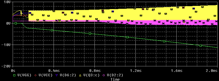
Voltage peaks on Q3's collector are a little above 6v, which rectified and
filtered by D8, C5 provides Vss 6Vdc. This voltage is doubled and inverted by
C4, D5 D7 and C6 to build -12 Vgg.
Finally, winding A gives Vcc around 8 Vdc via D4, C7.
Below, the probe screen after transient analysis.
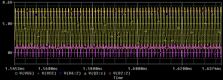
Below zoom on the pulses at Q3's base (purple) and collector (yellow).
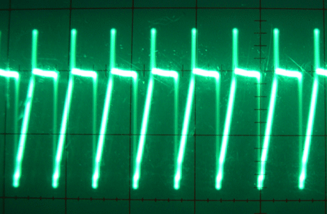
Below pictures are the Q3 base swing on the Pspice simulation and on the scope probing the real circuit:
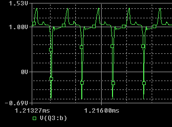 The pulse width is :
- calculated with the simulation around 1.25 us,
- extimated on the scope (time/div=2 us) around 1.2 us,
that means a frequency of 800 Khz that can be heard -in fact-
as a RFI in the MW band at 800 Khz.
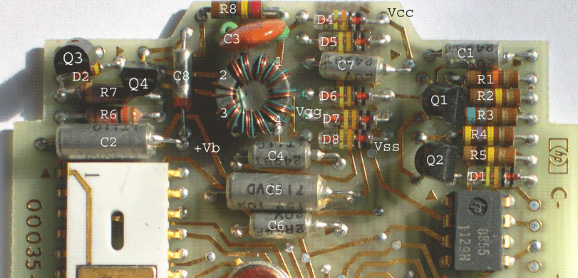
Below
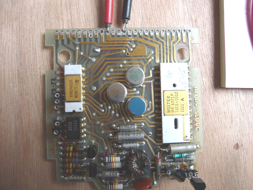
the components on the logic PCB, coherent with the Capture's schematic.
NB: R1 to R5, C1, D1, Q1, and Q2 are parts of the "power on" logic.
© Jacques Laporte
July, August 2008, Revisited and augmented Sept 2010.
Notes
(1)
PNP transistor model :
.model Q2N3702 PNP(Is=650.6E-18 Xti=3 Eg=1.11 Vaf=115.7 Bf=133.8 Ne=1.832
+ Ise=97.16f Ikf=1.081 Xtb=1.5 Br=3.73 Nc=2 Isc=0 Ikr=0 Rc=.715
+ Cjc=14.76p Mjc=.5383 Vjc=.75 Fc=.5 Cje=19.82p Mje=.3357 Vje=.75
+ Tr=114.1n Tf=761.3p Itf=.65 Vtf=5 Xtf=1.7 Rb=10)
* National pid=63 case=TO92
* 88-09-09 bam creation
NPN
transistor model :
* Model for 2N3904 NPN BJT (from Eval library in Pspice)
.model Q2N3904 NPN(Is=6.734f Xti=3 Eg=1.11 Vaf=74.03 Bf=416.4 Ne=1.259
+ Ise=6.734f Ikf=66.78m Xtb=1.5 Br=.7371 Nc=2 Isc=0 Ikr=0 Rc=1
+ Cjc=3.638p Mjc=.3085 Vjc=.75 Fc=.5 Cje=4.493p Mje=.2593 Vje=.75
+ Tr=239.5n Tf=301.2p Itf=.4 Vtf=4 Xtf=2 Rb=10)
.MODEL 1N34A D ( bv=75 cjo=0.5e-12 eg=0.67 ibv=18e-3
+ is=2e-7 rs=7 n=1.3 vj=0.1 m=0.27 )
(2) On the unit below, I have rebuilt completly the PSU.
Symptoms : unit not working, no Vcc, Vgg, Vss only Vbat (3.60Vdc) : Vbat at the
point where Vss should be (D8 K) signs always an oscillator problem.
I followed the following protocol:
I tested the junctions of each transistor, out of circuit (BE, BC and EC for
each).
tested the 7 diodes, and 8 caps C2 (60uf), C5 (22uf), C8(15uf), C3 (470pf), C4
(2.2uf), C6(2.2uf), C7(2.2uf), C1 ( 2.2uf).
(diodes in circuit testing is ok except for D2 - reverse bias, because of the
NPN's b-e junction in //)
I found
2 diodes and 2 transistors burnt out.
I replaced diodes D8 and D1 with Ge diodes 1N 60.
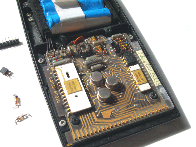
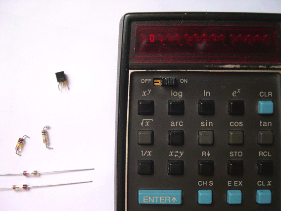
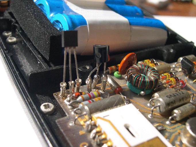
I constructed tripod supports for each BJT to make a few trials (see photo).
I tested 2N 3904 (NPN) and 2N 3906 (PNP), no way : the NPN is heating too much,
the PNP providing a too big current.
I tested 2N 3904 (NPN) and BC559C (PNP) : D8 exploded.
I tested 2N 3904 (NPN) and 2N 3702 (PNP) : bingo the pair started pulsing.
Finally I replaced the NPN Q3 (4-550) with a 2N 3904 and I replaced the PNP Q4 (3-020) with a 2N 3702.
But the 2N3702 is TO 92 B - "bce" - holes on the PCB are "cbe" and do not match - I had to twist the bc pins
(see third photo below).
Another way is to use MPS3702 which should be TO 92 A (cbe) hence PCB
compatible but difficult to find.
The unit is now working.
3) 11 6 2008 (revisited Sept 2010 - many HP35's DCDC fixed in 2 years)
Here are a few "good practices" for HP35 DCDC fixing.
Symptoms
of a dead DCDC : wrong voltage on Vcc, Vgg, Vss points, only Vbsw (3.6v).
The common case is the failure of D8 (Vss diode open) or D4 (Vcc diode open), or both.
I have found often
D8 "open" and Q3 dead (junction BE dead).
Diodes D4 and D8 are key parts of the oscilating circuit.
If
one of them is cut, the blocking oscillator stays in linear
operation : the PNP is providing its base current to the NPN that heats too
much.
On the scope, no pulsation on the base of Q3.
If no scope handy, your finger is enough : Q3 is heating a lot due to a high
collector current, Vbsw must be turned off or the Q3 (NPN) will be destroyed.
That's the fatal sequence, D4 burns -for a reason or another (age ....) - the PNP continues to provide current to the blocker that heats until thermal runaway.
I have reproduced the case, on my bench (I have a stock of burnt diodes to experiment). A 2N 3904 can stand up to 150°, my finger no! (If I remove the PNP the circuit does not oscillate but the NPN does not heat anymore).
In fact, it's a good rule of thumb : if no voltages but the NPN at normal temp :
the PNP is bad or the NPN is dead.
If the NPN is hot, the PNP provides current, the NPN is conducting at saturation
but the circuit is not pulsing : check the diodes D4 and D8.
The good working sequence to start is :
-
check all the diodes (should show around 0.250 on the digital multimeter - diode
mode)
- check the BJTs 'out of circuit' (the NPN gives wrong answers when tested in
circuit) ; "hello desoldering pump ...".
Black lead on base for the PNP, red lead on base for the NPN.
EB
and BC junctions of both BJT should show around 0.700 on the multimeter always in Diode
mode.
Reverse the meter
connections (on both transistors) to check that both PN do not conduct.
Finally check on both BJTs the possible 'open circuit' from emitter to collector - in both directions (Open circuit shows OL or 1 depending on the meter) ; a short can exist on EC even if each PN junctions tests ok.
This should cover 80%-90% of the cases.
After
that, if no avail, you will test the filtering caps:
- the big cap C2 (60uf) (may be good in value but high in ESR),
- C8 (15 uf).
It remains the rare but difficult cases. I remember an Australian HP65's DCDC with a steady Vss (6v) that was drooping when connected to the rest of the circuit and only in that case.
The culprit : corrosion on one ROMs pin that shorted current to ground. Desoldering pump etc ....
I have never had trouble with C3 and the pulse transfomer even if they are part of the circuit's heart.
Diodes 1N270, NPN 2N3904, PNP 2N3702 are perfect replacements (photo above both BJTs and D8 were changed).
4) Diode D2 identification.
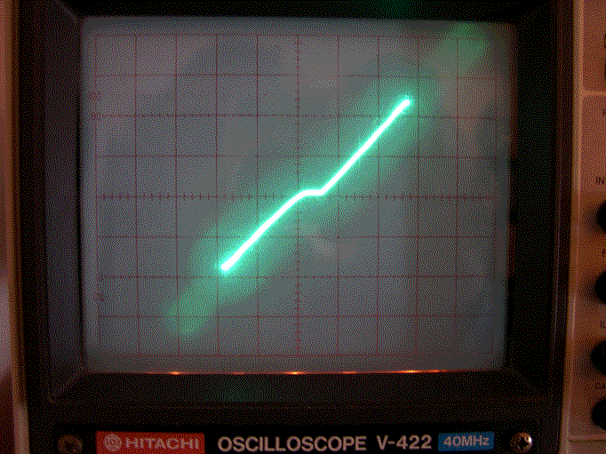
The circuit used to identify the diode D2 type on the HP-35 is simple:
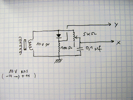 A
small transformer gives 10V RMS (in fact I took the wall charger of a HP25) : it
will sweep the range -14 +14 peak to peak.
The unknown diode is followed (cathode) by a 100 ohms resistor.
The RC cell 5k (pot) - 0.1uf is there to correct dephasing.
X-axis and Y-axis signals are applied to the scope in X-Y position.
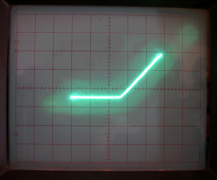
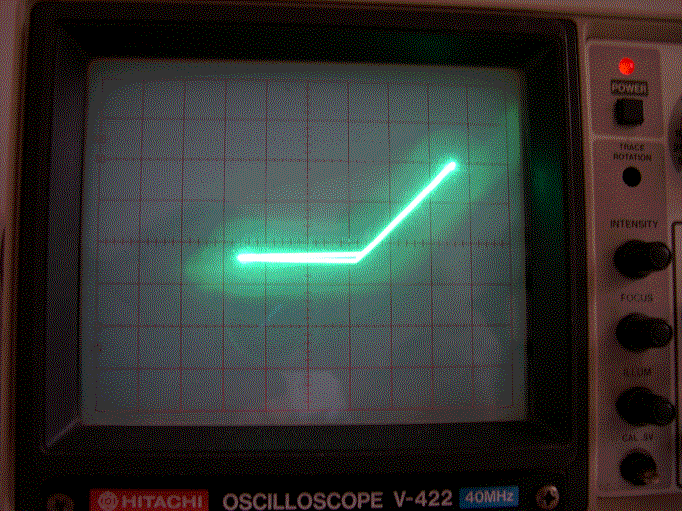
Below the screen pictures of the diode D2 -standard silicon diode curve- followed
-to ease comparison- by a genuine Zener BZX 85C 3.0V (break down knee voltage well visible)
and a standard rectifier 1N4007.
Conclusion : D2 is a silicon rectifier (forward voltage drop at 1ma is 640mV) used to protect Q3 emitter junction from destruction clipping the big negative part of the swing (-7 to -0.5v).
Below the D2 'unkown diode'
Example of Zener BZX 85C
Below : standard rectifier 1N4007
