The HP35's clock driver is a bipolar circuit (packed in
a 8 pin chip) that transforms the TTL clock provided by the Anode driver into a
clocking signal compatible with the PMOS circuits (A&R, C&T, ROMS).
Sources for the reverse engineering are : scope
analysis (input and output), HP patent 4001569 and Pspice simulation.
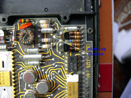
Below a general view of the circuit environnement : note the diodes D1 and D6 that are used to clamp to Vss (6vdc) the 2 MOS clock output Φ1 and Φ2. Both diodes disappeared in the more recent HP35 PCB (late 1973) probably integrated in the chip.
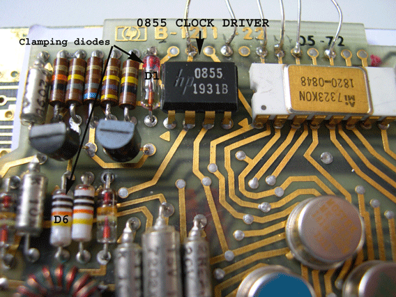
The next photo shows the pin out of the chip : Φ1 in
and Φ2 in are TTL signals from the Anode driver where they are built.
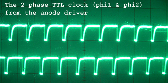
The 2 phase clock is created by flip-flops inside the Anode driver are ON for 625 ns
and are separated by 625 µsec, with a
800Khz main frequency.

The purpose of the Clock driver circuit is simple :
transforming TTL (0-5v) clock signal to MOS compatible clock signal (-12v 6v)
hence there are 2 TTL IN lines and 2 MOS OUT lines.
The next schematic has ben made with Orcad to run a PSpice simulation.
Note please:
- only one half of the circuit is shown (say Φ1 in and Φ1 out),
- V4 simulate the TTL clock,
- the right part of the circuit, clamping the output, is located outside the chip on early
machines,
- PNP and NPN are taken "out of the box" as 2N3702 and 2N3904 (they do not
behave exactly
like the genuine BJTs in the chip, but enough to understand the circuit),
- idem for diodes (1N4148).
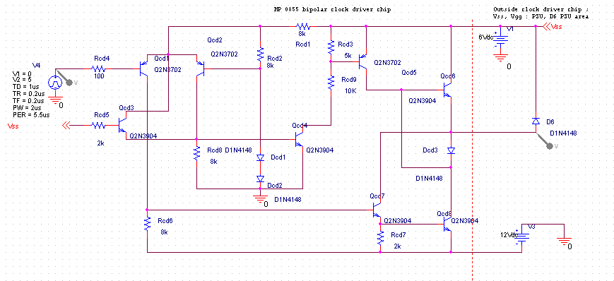
NB: reference to micro-components inside the circuit
are noted Xcdn (cd=clock driver) e.g. Qcd3 disambiguating with the general Q3
(HP35 main circuit).
V4 simulates the TTL clock (0v-5v) from Anode
driver(probe V(V4:+)) ; the output is the MOS clock signal, on Qcd6's emitter
(probe V(D3:1)).
Only one half Φ1 in and Φ1 out is drawn (see photos below).
The input Rcd5 - which is named "Enable" (98) in the Patent is connected to Vss,
and is used to "strobe" the clock (through Qcd3 and Qcd4, both on saturation, if
Enable is high and cut off if low).
On the HP35 the "strobe" input is not accessible from outside.
Transistor pair Qcd1 and Qcd2 is driving the "swing" of Qcd7-Qcd8 and Qcd5-Qcd6
: Qcd7 collector voltage and Qcd6 emitter voltage are the output.
When TTL = 0, Qcd1 is fwd active, its Vc = -10.5V drives Qcd7 and Qcd8 to
saturation hence Qcd7 collector voltage = -11.2V (Qcd8 collector = -11.7V).
Meanwhile, Qcd5 (Vb=5.2) and Qcd6 (Vb=-11.7, Ve=-11.20) are fwd active. Output =
-11.2V.
When TTL input is High =5V, Qcd1 is cutoff and its Vc = -12V hence the base of Qcd7
also ; it
drives Qcd7 (Ve=-12V) at cutoff, collector voltage is at 6V and Qcd8 is also cut
off (Vb=Ve=-12V, Vc=6V). Output= 6V.
During transient the diode Dcd3 prohibits reverse current. The Patent mentions
Qcd5 is a lateral PNP with limited current handling capabilitiy "less than 7ma
peak". The point is not simulated due to the lack of model for the BJT. A genuine 2N3702 is
taken for Qcd5, its current for TTL low is 50.8 ma.
HP claims the whole circuit requires less than 25 mw with a swing of +7 to -14V.
Anyway this study shows globally how the whole thing works.
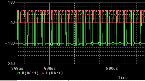
The result (Pspice probe) shows the TTL clock in red and the MOS swing in green.
In the real circuit the swing is wider (7v -14v) explaining the 6v clamping.
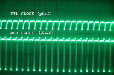
Below screen photo of a phase Φ2 TTL clock
(circuit input) and MOS clock (output).
Below screen photo of the 2 phases (Φ1 & Φ2) of
the TTL clock (output of the anode driver circuit).
Below a 1973 HP35 main pcb showing the two missing clamping diodes.
©Jacques Laporte
20008 Oct 21th.