|
|
HP-35 ROMs. |
The 3 HP-35 serial ROMs, in their T0-5 metal can, can be easily spotted on the photo below (photo by D. WEED).
See the beautiful hight res macro photos of the HP-35 ROM by P. Monta on his site and also on the forum.
Here is a low res photo of one HP-35 ROM chip, posted by P. Monta on the forum.
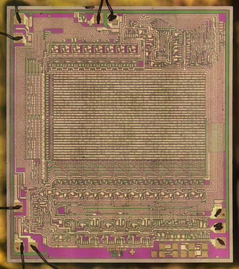
On this photo, the pins are : starting from top and clock wise : Vgg, Sync, Phi 1, Phi 2, Vss, Gnd, WS, Init, Is, Ia.
Center of the photo : the 32 rows by 80 columns = 2560 bit ROM array.
Each ROM contains 256 * 10 bit instructions (total 768 instructions on 3 ROMs).
The pin out is represented in the next schematic along with their link with A&R and C&T - respectively above and below the roms - on the PCB's photo:
- Pins 9 and 5 are Vgg and Vss respectively while pin 4 is wired to the ground,
- Pins 6 & 7 are providing the 2 phase clock ticks.
The 2 synchro signals INIT (& power on)
and SYNC (from the C&T) are inputs on pins 2 and 8.
WS (pin 3) is an output from one ROM to the logic, selecting a part of a
register.
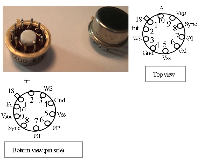
As usual, for a serial ROM, one pin is an address input (Ia pin 10) and another is an instructions output (Is pin 1).
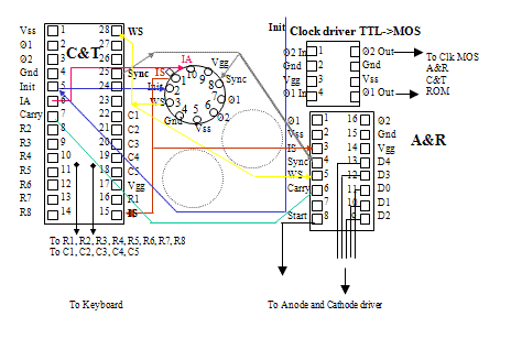
On figure 3, only one ROM is represented
since the wiring is the same (top view).
Figure 4 represents the ROM's internal
organization.
The 8 bit address register receives serial address from the C&T circuit and
gains access to the stored bits. A 10 bit instruction register transmits the
instructions bits serially to the outside (C&T and A&R).
There is no linear-selection scheme and no "chip-select" (CS) line ; so each of the 3 ROMS responds to an given 8 bit address but -of course- only one ROM has access to the Is bus, one at a time.
An enabling flip-fop is activating the right (1 in 3) AND gate giving access to the serial Is line.
This flip-flop is positioned :
- by the ROM select logic decoding the
"ROM select" instruction,
- or at Power on time, by the Init line (in the case of ROM 0) to insure
starting address is 0 in ROM 0.
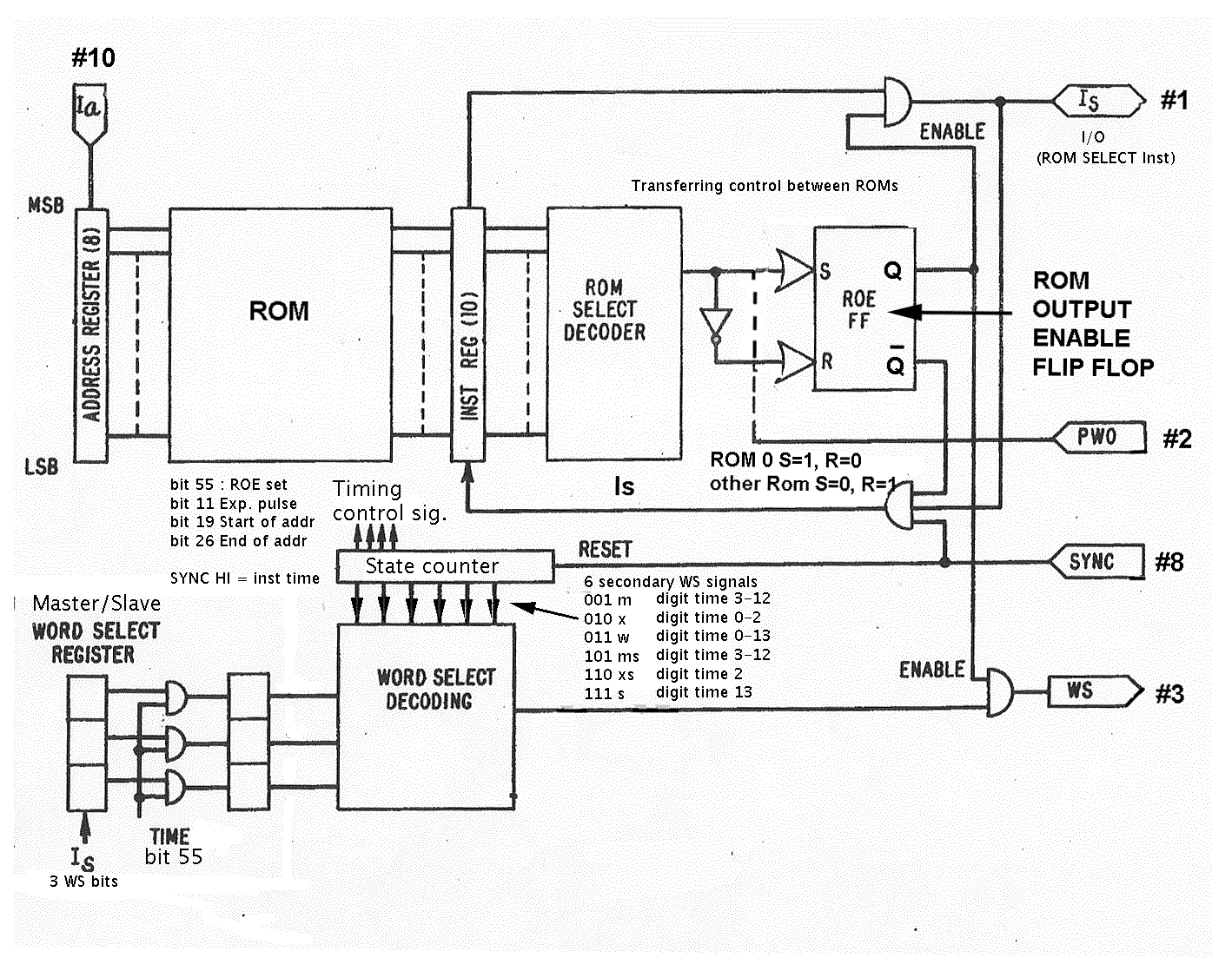
Note also, that the Is instruction flow circulates in the WS (Word Select) register to decode the WS part of instructions (if any) and send it on pin 3, to the C&T and A&R circuit.
The "Sync Counter" handles the synchronization of all of the 3 ROMs with the rest of the machine (C&T and A&R) : trailing edge of SYNC + one clock period is the start of the "word" time.

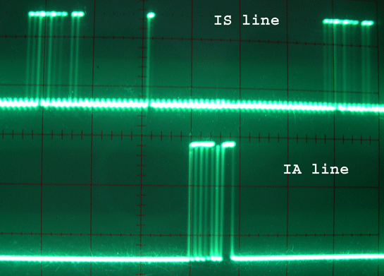
the IA line (8 bit address):

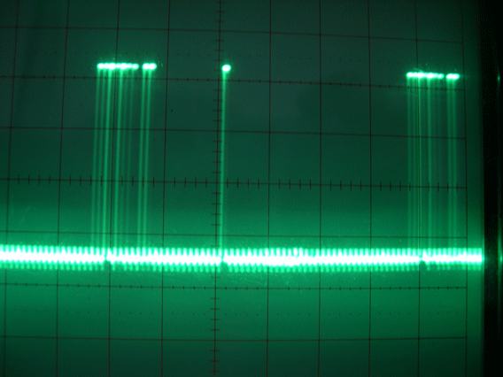
The IS 10 bit instruction word, note the 1 bit pulse (word time bit 11) used to decode the exponent minus sign time:
The 2 lines together:
©
Jacques Laporte
23/12/2009