|
|
HP-35 ROM dump |
In this article I will describe how to dump the ROM of a HP-35 (or another HP calculator) in half an hour and for a few dollars.
It sounds not serious, but in fact
reading the bit flow from the HP35 ROM is not very difficult to do as long as
you stick to a key-by-key approach.
That was my first attempt in 2006.
The next step is more difficult, since it required to remove the C&T and emulate
it with a micro controller putting on the "Ia" bus the requested ROM states (like a program
counter), reading instructions back on the Is bus and finally putting them in
the right order.
I will get back to this in a future article.
For now, the adresses (function entry points) requested are generated by a key press on the
keyboard and the instruction code flow is captured and stored on a PC.
The link between the HP35 and the PC
(Windows XP) is realized with the FTDI USB FT245BL chip as front-end hardware. I
bought an Elexol USBMOD4 kit available for 30
€ here in Europe. It offers a full speed - 8 bit parallel IO - ready to bake
USB.
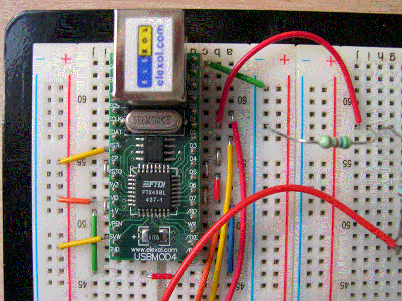
The configuration used is the Bus Powered one ; no external supply needed only a
common ground.
The software PC side is a simple VCP (Virtual COM) for a 300 Kbyte/sec speed ;
or D2XX (USB direct drivers + DLL interface for a maximum 1M byte/sec.
I used a free application DLP Design Test Application to store the flow -in this demonstrator- but VB (Visual Basic) or a C compiler could be used to develop easily the packing software (more on this later).
I will not enter in the theory of the USBMOD4 but
simply show the wiring to have it working with the HP.
It took me a couple of minutes to connect it to the PC.
- just put the kit on the breadboard (see photos), there are 32 pins named on the
PCB,
- strap pin 9 and 10 (named EP and RSTO),
- strap pin 12 and 13 (named VIO and V+), Device Vcc (no external connection
needed),
- connect V+ to the Vcc red line of the board,
- tie pin 8 RSTI to Vcc red line,
- tie pin 15 SI/W to Vcc red line (see photo),
- make on the board a HIGH line form V+ (green + red + blue straps) to have the
Logic 1 on the 8 bit side of the kit,
- connect pin 32 (device gound) to the blue line of the board (common gound with
the HP),
- make a [11111] pattern on the 5 most
significant bits (msb) of the 8 bit word,

We will connect d2, d2, d0 respectively to the SYNC, Is and Ia of the HP-35.
But first let's make a pause to avoid possible problems and let's test the usb
connexion alone.
Bring Logic 0 (gound) to d2, d2, d0. If all is ok, the FT245 will send
[11111000] (Hex F8) to the PC.
We need a WRITE pulse, let's make it crudely by stealing it from the
"/TXE" line (when going low data can be writen to the FIFO) ; just strap pin 18
/TXE and pin 19 WR (Transmit FIFO when WR goes from high to low).
If you need more help, refer to Eddy INSAM, "USB made easy", Electronics World
Feb 1972, p.52.
Launch the "DLP Design Test Application" on the PC, connect a USB cable between the PC and the USBMOD4 kit. Select DLL, open the Port and now the data "F8" start to run on the "Receive Data" Window.
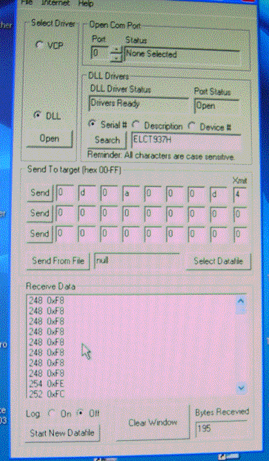
If all is ok at this step, you're on the
right track.
You probably have understood that each byte sent will pack the
state of SYNC, Is and Ia lines, for each HP-35 clock pulse.
Now the link between HP-35 and
USBMOD4 kit.
I was very lucky the evening I designed that experiment : HP-35 has P-MOS logic
0-6V and the USBMOD4 kit need TTL logic (0-5V) ; but a quick and dirty resistor divider
(2.7k + 5.6k to ground) did it.
The Mos clock has a -12/+6V swing, I first put a diode before the resistor divider on the clock line to clip the negative half, but finally I removed it since the USBMOD4 works well without.
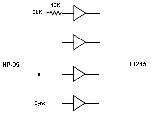
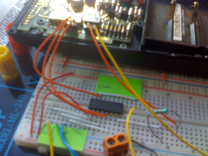
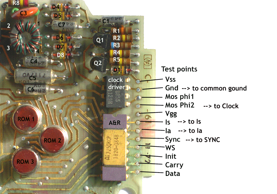
Let's get the things together : 4 lines
with resistor dividers, Clock, SYNC, Ia and Is and a common gound, connected on
the test points of the HP-35 (see schematic) and on the USBMOD4 kit :
-
Clock to WR (Write) pin 19,
-
SYNC to d2 pin 26,
-
Ia (address) to d1 pin 27,
-
Is (instruction) to d0 pin 28.
Ground from the HP-35 to blue line of the board.
If you want to build a more robust interface, you should use CD4050 non inverting CMOS buffers between the calculator and the FT245, to have a clean TTL signal ; the MOS clock swing should be reduced by a simple 33K-40K resistor, before the buffer input.
The data dumped to a the file by
the application speaks by itself :
Hex FE means
[11111110] =>
SYNC=1, Is=1, Ia=0
Hex FC means
[11111100]
=> SYNC=1, Is=0, Ia=0
Hex FA means
[11111010]
=> SYNC=0, Is=1, Ia=0
Hex F9 means
[11111001]
=> SYNC=0, Is=0, Ia=1
Hex F8 means
[11111000]
=> SYNC=0, Is=0, Ia=0
We can check on the listing the two time windows
;
- between b19 and b26: the 8 bit address is active on the bus (Ia line),
- between b45 and
b54: the 10 bit addressed instruction is active on the bus (Is line) strobe SYNC
High,
- bit 11, used by A&R to decode the exponent minus sign time
(Hex FA).

Excerpt of the dump file (one word):
Format of the 8 bit word received from USB is <dec data, hex data> (I have added the bit number 0-55)
248 0xF8 0
F8 = 11111000 = NO SYNC, Is = 0, Ia = 0
248 0xF8 1
248 0xF8 2
248 0xF8 3
248 0xF8 4
248 0xF8 5
248 0xF8 6
248 0xF8 7
248 0xF8 8
248 0xF8 9
248 0xF8 10
250 0xFA 11 FA =
11111010 = NO SYNC, IS = 1, Ia = 0
248 0xF8 12
248 0xF8 13
248 0xF8 14
248 0xF8 15
248 0xF8 16
248 0xF8 17
248 0xF8 18
------------------- F9 = 11111001 = NO SYNC, Is = 0, Ia
= 1 ; below 8 bit addr pattern
249 0xF9 19 1
248 0xF8 20 0
249 0xF9 21 1
249 0xF9 22 1
248 0xF8 23 0
248 0xF8 24 0
249 0xF9 25 1
249 0xF9 26
1 address is "11001101" = 315 octal
(LSB comes first)
------------------
248 0xF8 27
248 0xF8 28
248 0xF8 29
248 0xF8 30
248 0xF8 31
248 0xF8 32
248 0xF8 33
248 0xF8 34
248 0xF8 35
248 0xF8 36
248 0xF8 37
248 0xF8 38
248 0xF8 39
248 0xF8 40
248 0xF8 41
248 0xF8 42
248 0xF8 43
248 0xF8 44 FC = 11111100
= SYNC, Is = 0, Ia = 0
------------------ FE = 11111110 = SYNC, Is = 1, Ia = 0
; below 10 bit instruction pattern
252 0xFC 45 0
252 0xFC 46 0
254 0xFE 47 1
252 0xFC 48 0
254 0xFE 49 1
252 0xFC 50 0
252 0xFC 51 0
252 0xFC 52 0
252 0xFC 53 0
252 0xFC 54 0
instruction is "0000010100" = 24 octal ; instruction "if s = 0"
------------------
248 0xF8 55
We can immediatly compare with the ROM listing.
We've just captured the flow in the "wait a key" loop at address 00315 octal, label dsp5, the code is
testing if a key has been pressed. At that time the screen of the calculator was
"0."
.../...
L00314:
0000101000
dsp4: display toggle
L00315:
0000010100
dsp5: if s0 = 0
L00316: 1100011111 ->
L00307
then go to dsp3
.../...
Obviously to read a whole function flow, some code is required to do what we
have done by hand : pack and invert address and instruction bits (synchronized
by SYNC - F8 and F9 = address - FC and FE = instructions).
Selecting correctly the functions on the right data, it is possible to walk
through the entire ROM set : there is always a path (and a minimal key strokes)
to cover 100% of the ROM states (even if not straightforward : for example "overflow" or
error cases).
November 11th 2008
© Jacques Laporte 2008.
All photos J. Laporte
NB:
This
approach was taken -for the first time, as far as I know- by Tom NAPIER,
back in 1978, in his article "An HP-67 Anatomy Lesson" PPC JOURNAL V5 N7 Page 8
Aug 78.
Tom used two 74164 serial to parallel converters to interface a HP-67 with a
8080 microprocessor system, fetching ISA and DATA bus signals, 7 bits at a time
and storing the flow in RAM before printing it out.
Tom published in the same PPC Journal (Nov 78-Dec 78) a few commented micro instruction listings for a set of selected operations keyed in at the HP-67's keyboard.