|
|
HP-35 Display system |
In this article (4 pages) I will describe the display and keyboard system of the HP-35 and other Classic calculators.
Light-emitting
diodes (LED) were commonly used, at the very start of the 70's, to
output status and other information to the user of a calculating
device.
Displays were arranged in seven-segment clusters or in
dot-matrix blocks.
But the 1971's state of the art red LED technology was excessively power consuming.
The TTL command through the base of a NPN transistor induced a typical current of 10 to 20 millamps through the emitter resistor and the diode.
1) Principle of operations
For the
HP-35, the
DC current feed system has been abandoned and the LEDs were operated in a low duty pulsed mode rather than continuous.
An "anode" NPN transistor is driven into conduction by a
pulsed signal applied to its base and its collector
is loaded by an inductance ; the LED is connected across the
inductor and is forward-biased shortly when the transistor is at cut
off, producing light at a low current consumption. In this
manner, there is no current-limiting
resistance in series with the LED the no power
dissipation into it. The
energy is first stored in inductors and dumped into the
LEDs, in the second part of the cycle.
For one segment : when the pulse is positive, the anode transistor is on, causing the current to build up into the inductor. At the end of the pulse, the transistor is off and the current flows into the LED, causing the light emission.
This approach was new and revolutionary in 1971 for the HP-35 and the Classic series (HP-45, HP-55, HP-65 ...). HP presented as a discovery the fact that -at that time- the LEDs available show greater efficiency producing light when forward-biased in a pulsed mode. Amplitude and repetition rate are determined so the light pulses appear continuous to the eye of the user.
Note,
that the "inductive" scheme has been abandoned in the nest generation
'Woodstock' as LSI and LED technology evolved.
The
sketch below represents the principle of operation : a red LED "digit"
is made of 8 segments (Sa, Sb, Sc, Sd, Se, Sf, Sg and a
decimal point Sdp) ; each segment is a LED connected as shown - anode
to inductor and 'anode' transistor's collector - cathode to the
'cathode' transistor's collector.
There are 15 characters in the HP-35's display then 15 cathode
transistors.
 Pulses
are around 2.5us large and the current builds up to 80ma ;
then it decays during 6 us through the LED.
Each segment is pulsed every 280us for 2.5us ; the duty cycle is about 0.9% (the machine time word is 280us).
The major point to catch is the each "segment" (couple NPJ + LED) are pulsed and each "digit" or cathode (8 segment block) are pulsed too, swept sequentially, one at a time, one segment at a time.
The 8 'anode' transistors are arranged in a bipolar LSI chip : the "anode driver" while the 15 'cathode' transistors are packed in a chip driven by a shift register : the "cathode driver".
A signal
'STEP' is provided by the anode driver to advance the cathode driver to
the next digit.
A signal 'RCD' (Reset Cathode Driver) is provided each 280us, by the calculator logic
(A&R) to reset the cycle and do the scanning over again.
To be complete, as we will see in detail, the "digit time" (each segment) of the time word is multiplexed to a high degree.
The digit time word is 20us, then 280/20=14 the calculator word cycle is 14 digits long ; the extra character being the decimal point (more on this later).
To get
things together, there are 4 important points :
-segments are pulsed (2.5us pulses),
-cathodes are sequentially selected (signal STEP),
-sweep is reset by a RCD signal each word time (280us),
-segments
pulsing is multiplexed (Se, Sg, Sc, Sa ..).
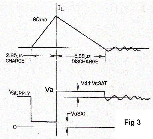
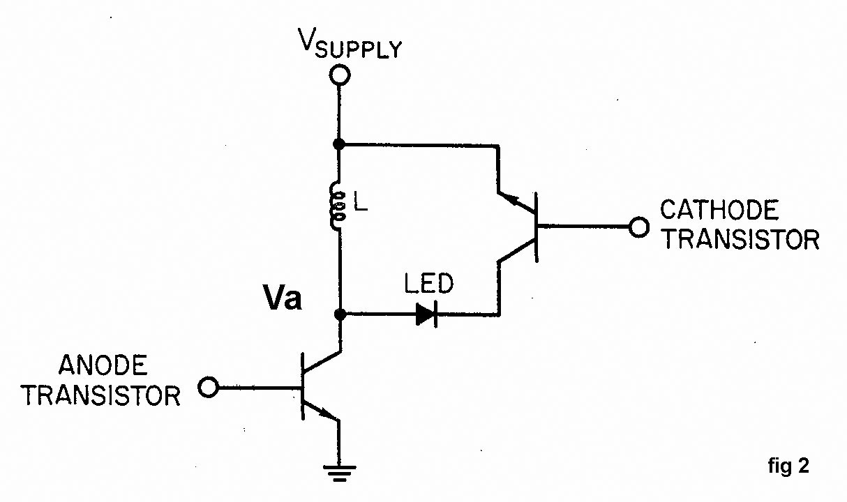
On the fig 2 is represented the electrical diagram, and fig 3 shows the current form
in the inductor.
When the anode BJT is ON
(base close to VaSAT= 0.3V), the current is building up
in the inductor
for 2.85us
up to 80ma.
When the anode
BJT is OFF
(Vd = 1.7V Led
drop + VcSAT = 0.45 together around 2.15V), the current decays through the LED, for about 6us,
transforming energy
in light.
(VaSAT = saturation voltage of Anode BJT, VcSAT is saturation voltage of Cathode BJT).
The decay time is 2 times the build up time, that is 80ma anode current, 250 ma cathode current but for short periods of time.
On the real calculator anode BJT
are packed in the anode driver chip, but the point
VA
does exist outside and links the chip to the inductor.
The LEDs are packed in 5 digit clusters.
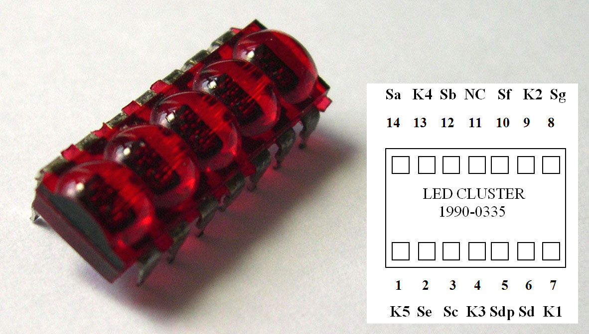
As mentioned above LED's segments are excited in a pulsed mode, but they can be tested easily in direct mode providing a resistor to limit current. If we put 3.6 V DC '+' (from batteries) on pin 14 of a Classic LED cluster (Anode a) through a 100 or 200 ohms resistor (on the photo I took a 82 ohm) and the negative polarity on pin 7 (cathode 1), we light segment 'a' on the first 'digit'. These Leds forward drop is around 1.7 V, so the current across the segment is = (3.6 - 1.7) / 82 = 23 ma ; explaining the brightness : 200 ohms should be safer.
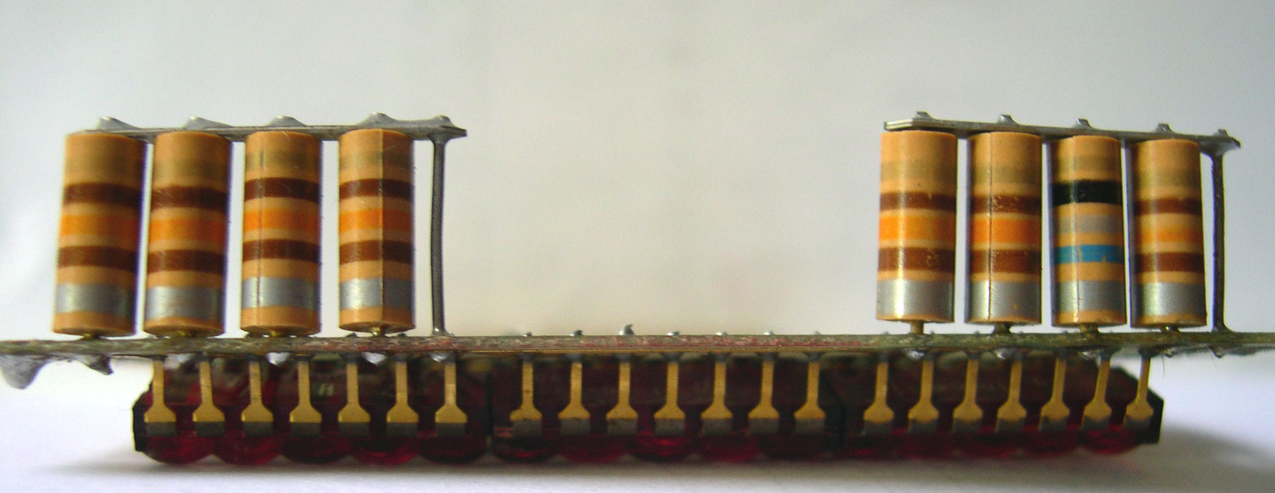
Each inductor has a value of 130uH except decimal point 68uf.
2) Segments multiplexing
As discussed in the relevant part, the display is partially decoded in the A&R register which outputs its display data, to the anode driver on 5 lines (A, B, C, D, E ) on pins 9 to 13, to address 8 segments + the decimal point.
To deal
with this, segments are multiplexed during the 20us digit time which is
divided in 4 part of 5 us each, T1, T2, T3, T4.
(digit time T1 to T4 is 20us large ; 14
digits in a 280 us word time.).
The
"basic" 7 segments 'a' to 'g' are excited during T1, T2, T3 while the
decimal point is emitted during T4.
All the inductor current must be decayed before the STEP signal is emitted.
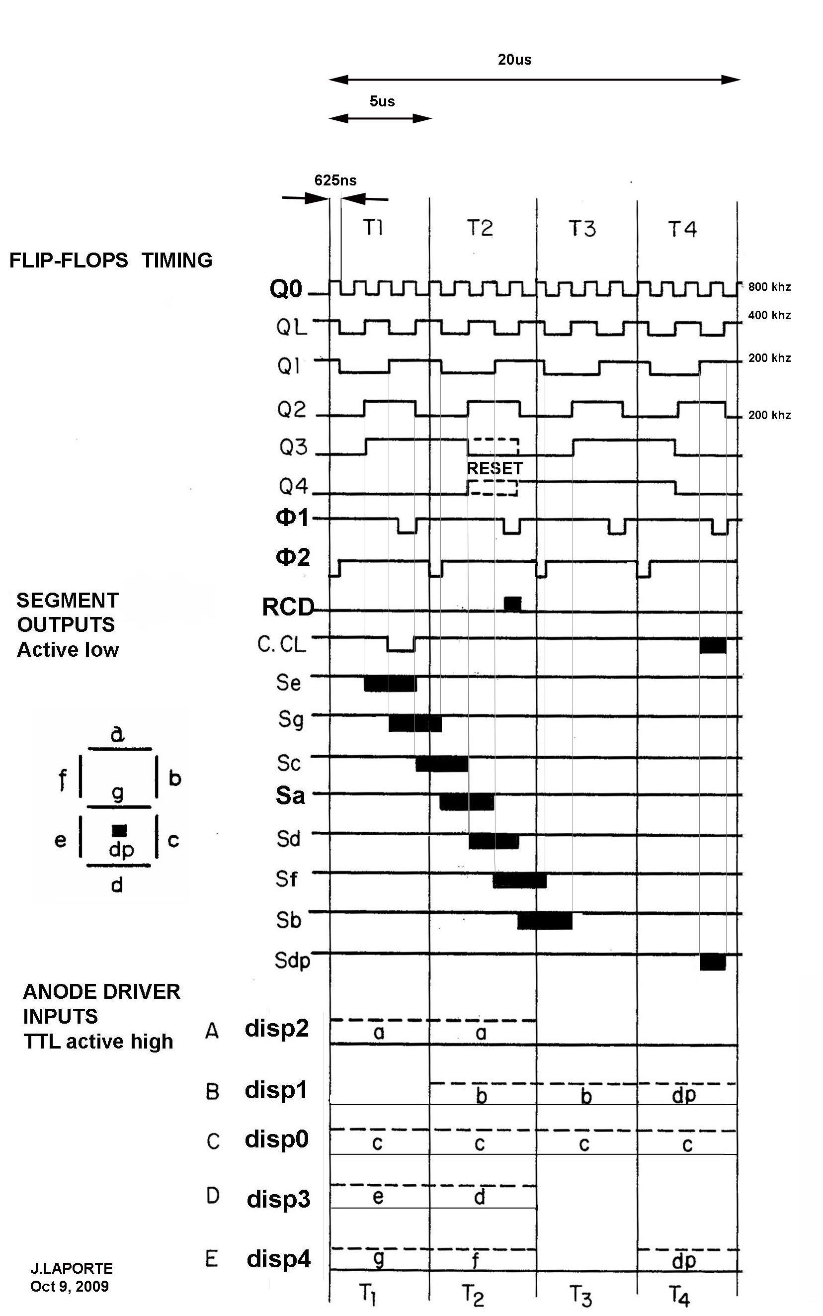
The timing diagram below shows the relation between the master clock Q0 (around
800khz) and
the 'segments' pulses.
8 segments 5 data lines : segments Se, Sd, Sg, Sf et dp are time shared.
On a cleared 'CLx' display, pressing key '1' will form the following display "1." : the signals needed are segments 'b', 'c', STEP and "dp". That is logical 1 on line B during T2 & T3, logical 1 on line C T1-T4, and logical 1 on line B during T4.
After
an interval of 280us the same pattern is pulsed again and so on..
Note
again, RCD = 625ns during T2 (reset cathode sweep).
On the timing diagram below, I reproduced
-the flip-flop timing (10 first lines) in the anode driver that switch the
inputs lines from A&R,
-the TTL
signals (lines A to E) from the A&R,
-the signal to the anode transistors (active low)
exciting the segments (8 middle lines Se-Sdp),
width 4 times 625ns = 2.5us.
These data are extracted from the US patent 4001569 (HP45) but corrected as many
typos or errors were left in this
document.
A simple way to test the display timing is to bring swiftly, on the anode driver the voltage Vcc (pin 11) to pin 1 (d0), 2 (d1), 3 (d2), 4 (d3), 5 (d4) : the corresponding segments can be checked (photo below).

It is
also a convenient way to test the cathode driver, since each pattern
(e.g. Vcc on d3 lights sd and se, Vcc on d2 lights segment 'a') is propagated on all digits.
On the photo (left) Vcc (red grip-pin
11) is wired on d2, pin 3 of the anode driver.
The consequence is that segment 'a' is lit in complement of the digit segments '0.' lit by A&R.
Note that those extra segments are propagated
automatically on all the digits by the STEP signal.
A convenient way to test both anode and cathode drivers.
My next experiment was to catch on the scope photo the 8 segment signals on the first digit, or at least a sample.

Wish I had an improbable 5 channel Scope or a logic analyzer!
I have done my best to take
clear scope pictures.
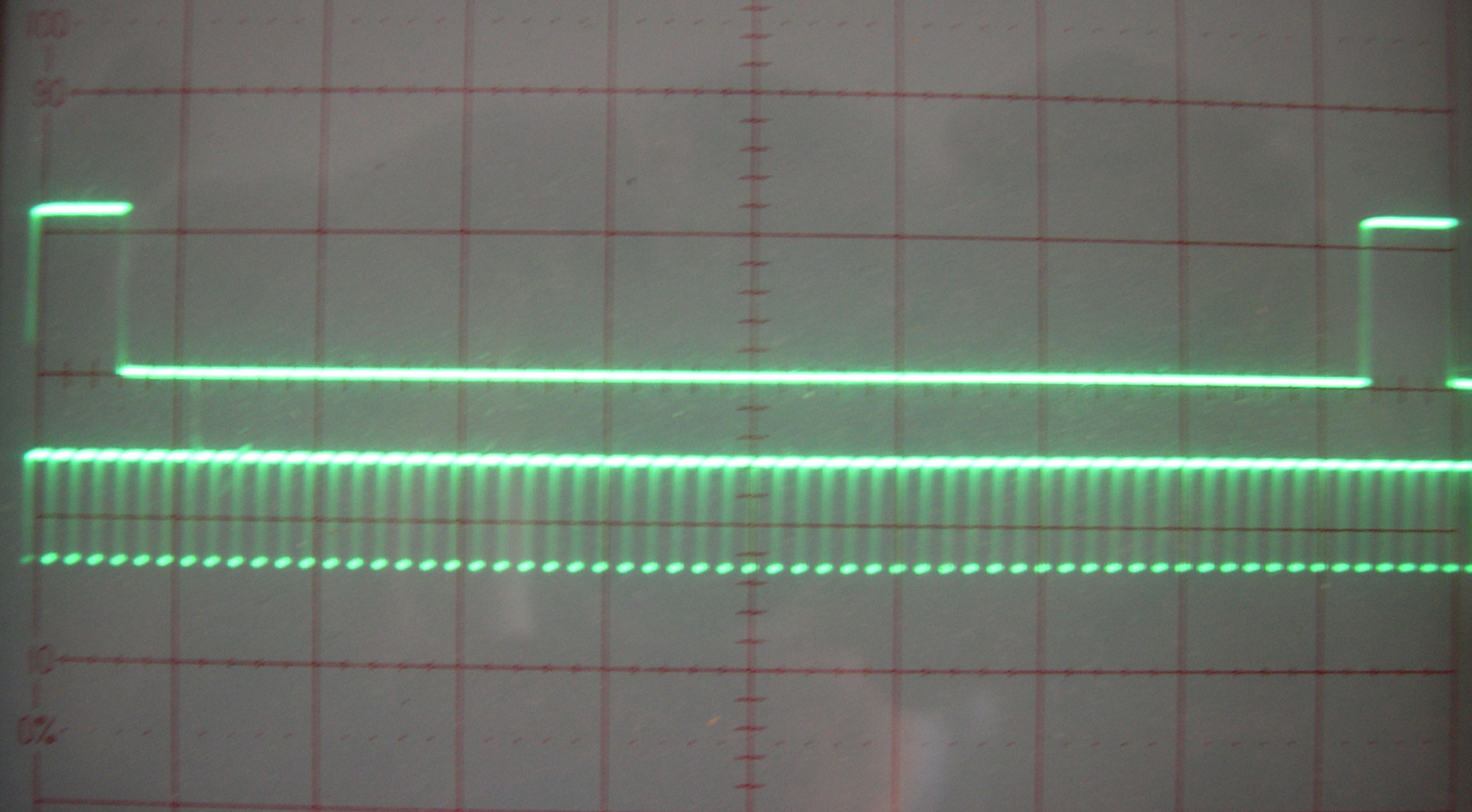
Digit '1' on the display.
On the first photo below, I caught the pulse
on disp0 (upper trace) during the time window from T1 to T4 : that's segment c
(the lower part of digit '1', the upper part being segment b). To establish a
time-base, I put the second channel's probe on Ø2
(lower line).
Clearly, we see the 56 bit time word and the pulse on disp0 during four Ø2 pulses (time window T1-T4).
The next photo was taken a probe on disp0 (line C) and another -the other channel- on the Anode C (Inductor L3 on my schematic diagram) ; I enlarged it to show the details, the upper signal (disp0) is 20us (3.8 div):

The disp0 TTL input pulse (line C) is lasting from T1 to T4 (20us), the output signal
for Segment C (Anode C) starts (see timing diagram above) at the end of T1 and ends at the middle of T2 (width
=4*625ns=2.5us) ; the inductor beeing charged during 2.85us.
Line C is not time shared and it is the job of the anode driver
(through its flip-flops and gates) to switch and excite the right anode according to timing.
The next photo shows signals on Anode A and on Anode D (upper and lower horizontal segments used for figures like 0, 3 or 8 etc..) ; Anode D is excited 1.25us (2*625ns) after Anode A. It is clearly visible on this beautiful pic taken on a digital scope by my friend François Roulet, with my thanks, (anode A first line, anode D second).

More photos soon.
J. LAPORTE, Aug 20, 2009 Oct 6 2009.