|
|
HP-35 hardware basic design |
The purpose of this paper is to present the basic hardware design of the HP-35
The HP 35 is a bit-serial calculator organized to process 14-digit BCD words.
To clearly introduce this concept (which is not new in 1972), I will refer the reader to the text of the only patent concerning the HP-35: US Patent N° 3,781,820, granted to D. Cochran and T. Osborn (files May 90, 1972).
Although the HP-35 is just named therein a “portable electronic calculator”, 3 key inventions are well described: the stack with automatic push or pull, the ENTER key, and the CHS key.
This patent is obviously expired, but it keeps its great pedagogical interest.
One warning first: it is a “flip-flop and
gates” description and not the real implementation realized with two level of
micro-code:
- a micro-sequencer
- 3 Roms.
The HP-35 has a “bit-serial architecture” that is to say that all data circulating on the 3 main lines of its bus are “serial”; so timing considerations are crucial.
 The
basic clock frequency of the system is given by a simple oscillator driven by a
LC cell (no crystal) ; the clock rate is 200 khz (800 khz divided by 4) so the
bit time width is 5 μs and the digit time width is 20 μs (5 * 4).
As the serial word is a 14 digits word (mantissa 10 digits - exponent 2 digits,
mantissa sign (1 digit) and exponent sign (1 digit) , the word time is 56 bits
(14 digits * 4 bits).
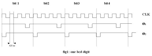
Fig 1 shows the
timing for one BCD digit (4 bits):
During the bit time of 5 μs, 4 clock pulses of 625 ns each can be counted.
This timing -that rhythms the life
of the machine- is created in the Anode driver circuit, together with the
signals to drive each one of the 8 segments of one LED and the signals to
synchronize the cathode driver (reset and step).
 All
this logic uses a TTL technology (mainly 5 flip-flops, 15 “and” gates, 3 “or”
gates).
The clock signal delivered to the rest of the machine consists in a 2 phase clock (separated by 625 ns) consistent with the PMOS technology used in the main chips of the calculator.
A circuit named
“clock driver” converts the TTL clock levels to the MOS technology logic
requirements.
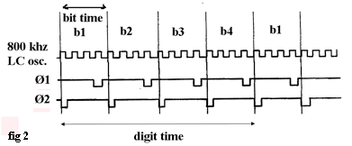
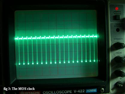
Fig 2 above shows the BCD digit timing (4 bits) and fig 3 below shows the MOS
clock (a swing from -12V to +6V.
Now, I return to the
serial bit paradigm described in the patent n°
3,781,820.
I suppose there are 4 word times (multiples of the 56 bits word time) defined to
correspond to the presence of the machine word in the register KB, M1, M2 and M3
of the calculator’s stack (that’s in the real implementation X, Y , Z, and T).
I simplified a lot the main diagram (fig 4) but it’s enough to understand 2 main things in the architecture.
In order to make Y (MI) and X (KB) available simultaneously a one-word time early tap 164 is provided on the stack.
(here I’ll follow closely David Cochran):
- during WI, gate 62 is closed and AND gate 92 is opened to pass KB into ADDER 90,
- at the same time AND gate 94 is opened by AND gate 96 to pass MI into ADDER 90, where the contents of KB and M I are combined and put on line 160.
- during W2 and W3 gate 92 is closed but gate 94 is left open pushing up the contents of M3 and M2 to M2 and M I respectively.
- during W4 gate 94 is closed and gate 62 is reopened leaving the contents of M3 unchanged so that M3 and M2 then contain the same data.

Finally, you’re now able to catch a main point: in this kind of calculator, the data is dynamically and constantly re-circulated into the registers.
I advise to download
the document and follow each path for digits entry, “ENTER”, “STO”, RCL” etc…
Remember the pattern describes a “flip-flop and gates” implementation as the
real implementation is made with a CPU and 3 Roms.
You can understand
now that why the serial registers of the Arithmetic Unit are 56 bits wide. The
precise timing of the word time is given by fig. 5.
Two time windows are
remarkable.
- Between b19 and b26: the 8 bit address is active on the bus (Ia line)
originating from the control logic of the system (Control and Timing circuit) to
be read by the ROMs : only one of the 3 ROMs is active at a time,
- between b45 and
b54: the 10 bit addressed instruction is active on the bus (Is line) from the
selected ROM to the Arithmetic and Register circuit, to be decoded and executed.

The “strobe”
synchronizing the system (SYNC) is issued by the C&T during the window b45-b54.
No other strobe is available and the ROMs are keeping the pace using their own
synchronized 56 bit counters.
Two other lines form the system bus:
1) WS (Word Select)
is issued from the C&T and from the ROMs to A&R enabling instructions to be
executed only on portion of the word (exponent, mantissa, exponent sign etc.)
The pair C&T and A&R forms a very specialized CPU compared to the early
microprocessors available in 1972 (e.g. Intel 4004).
2) the Carry line which task is to report a carry condition from the A&R to the
C&T (to be used in arithmetic and by the “goto if n/c” instruction, for
example).
Now I will open 3 other “black boxes” that I will detail more and more, as my
description follows.
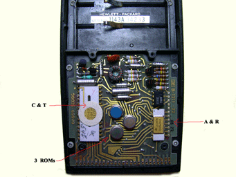 The
core of the system consists of
-
the Control and
Timing Circuit (C&T),
-
the Arithmetic
and Register Circuit (A&R),
forming together the specialized CPU,
-
3 ROMS of 256
bits each, containing the firmware.
I will let apart (to
get back to them later in details):
- the clock generation circuits (for now it’s enough to know that the 5 MOS
devices (C&T, A&R and ROMs) are fed with the right 2 phase clock signal),
- the LED display
logic -anode and cathode- (and consider that with 5 lines output of the A & R
circuit we know how to display the 10 digits and the decimal point),
- the power supply unit and the power on logic,
Fig 6 Simplified diagram

I will focus on the main parts: the C&T, the A&R and the Roms.
Figure 6 gives a first schematic diagram.
The C&T and A&R can
be seen as one function : the processing unit. In fact, in the next generation
(Woodstock), they were packed in one chip.
(fig 7: C&T chip)
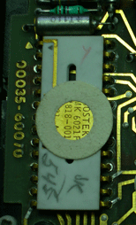 The
C&T is the control unit of the system ; it has the following tasks:
-
operating
instruction counter and saving the return address,
-
keeping the
status bits,
-
scanning the
keyboard (8 rows x 5 columns),
-
handling the
pointer P,
-
synchronizing the
system (SYNC and WS signals)
Note that the HP-35 follows the Wilkes' model and that the C&T is microprogrammed.
A 1450 bit control
ROM (58 words * 25 bits each) is used to generate the signals to control the
data flow, reacting to qualifiers (PWO, timing, carry flip/flop etc.) ; each bit
of this ROM correspond to (or is part of) a signal control line.
This is the most secret part of the system though one can “guess” the way it
works.
(fig 8: A&R
chip)
 The
A&R is the arithmetic unit and its main tasks are:
-
decoding and
executing instructions on registers (the ALU is not orthogonal
(an instruction set is said to be orthogonal
if any instruction can use any register)
and certain instructions
operate only on certain registers),
-
handling the adder,
-
handling the 7 register stack,
- outputting the data to the display module (5 lines).
As we have seen
above 4 lines are inking these 5 units:
- Ia (Addresses) C&T -> ROMs
-
 Is
(Instructions) ROMs -> A&R (and to C&T for « return addresses »),
- SYNC
which is the strobe signal synchronizing the 5 unis,
-
WS (Word select)
which select a part (field) in the 56 bit word,
- a carry line links the A&R to the C&T.
With a basic “word time” rated at 280μsec the HP-35 is a fast small computer but slower than its predecessor the HP-9100A.
The HP-35 is made of MOS LSI circuits (a brand new technology in 1972) ; the HP-9100 is made of discrete components (diode and bipolar transistor logic).
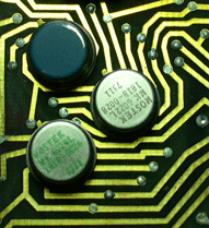
(fig9: The 3 ROMs)
The memory core access time on the 9100 is around 5 μsec ; on the HP-35 ROM access takes place between bit 27 and bit 43 of the word time (85 μsec), 17 times slower than the 9100.
Comparing processors is difficult, since the clock makes each processor do something each cycle, but what that it does can be significantly different. A comparison makes only sense at the operation level when the algorithms are close:
HP-35
- floating point “+” and “-“(215 word times) = 60 ms,
- floating point “*” and “/” = 100ms,
- digit by digit ln and ex = 200ms,
- CORDIC trigo (tan, sin, cos) = 500ms.
HP-9000A
- floating point “+” and “-“= 2 ms,
- floating point “*”= 12ms,
- floating point “/” = 18ms,
- digit by digit ln = 50ms,
- digit by digit ex = 110ms,
- CORDIC trigo (tan, sin, cos) = 280ms.
If I take as a norm the FP multiplication time the HP-35 is only 10 times slower
than the 9100A.
To give comparisons:
- the
floating point multiplication takes 6 seconds on the Harvard-IBM 1946 Mark I,
and 450 μsec on the 1953 IBM model 701),
- the IBM System/360 Model 91 was introduced in 1966 and was the fastest, most
powerful computer then in use. The NASA operated a Model 91 in 1968 at Space
Flight Center in Greenbelt, Md ; at the same time the HP 9100A was introduced
(Barney Oliver initiated the HP 9100A project in late 1965).
The machine executed up to 5,530,000 floating Point multiplications per second:
180.83 nsec each.
Another point of comparison is the CORDIC itself; developed at Convair, it successfully passed radar fix-taking test in 1962. The Model B specially made for airborne operations was a 30 bits, bit serial, binary computer with a time for multiplication or CORDIC operation of 5ms. Jack VOLDER wrote recently that only 5 B-58 bombers survived (with their Cordic, I presume) in aircraft museums.
Finally, note that Hewlett-Packard
laboratories built in 1970-71 a high speed hardware 12 decimal digit floating
point processor based on Cordic (8 bit parallel adder/subtracter) and controlled
by micro program
in ROM.
The execution time was impressive:
- tangent= 130 μsec,
- logarithm= 70 μsec
(fig10: SYNC signal)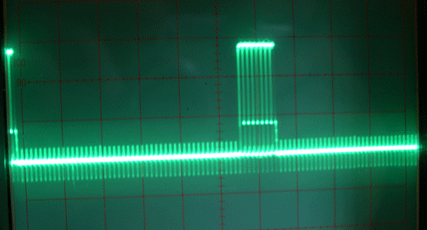
Here is now a small story board of the operations, starting at power on.
A power on circuit
(a 2 bipolar transistor and 5 resistor one shot) forces the system in a clean
and known condition.
It sets the starting 8 bit address octal 000 ROM 0 and gives time to the system
56 bit counter to be synchronized with the 56 bit counter in each ROM
This is done by just holding the PWO signal at logic 1, in order to have the counters synchronized and the ROM 0 selected.
The first
instruction at address 0000 in ROM 0 must be a “go to” or a “call” (PWO routine)
and operations can begin.
(fig 11: The 2 time windows, address and instructions (with Sync)
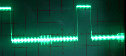
I’ll give more information on this later, but note that addresses are relative to the selected ROM (one among 3).
The address buffer is 8 bit large and the C&T can address linearly the range 000-377 (octal).
So in each ROM there is an « enable » flip flop mechanism that decodes itself a «select ROM x » instruction: the right ROM is ON the others OFF.
For example, the code for key “1/x” starts at 0016 (rom 0) – see listing - if we capture the signal on the Is line, here is what we will see (key “1/x” actuated):
address opcode
0001110: 1011101110
0 -> a[w]
0001111: 1111100010 a + 1 -> a[p]
0010000: 0000101110 0 -> b[w]
0010001: 0010010000 select rom 1
0010010: 1010011001 jsb 246
0010011: 1010010100 if s10 = 0
0010100: 1101101011 then go to 332
the first 4 instructions are in rom 0 and the last 3 are in rom 1 (the 2 targets 246 and 332 also).
Fig 10 shows the SYNC signal, while Fig 11 gives an insight of the two HP-35’s “time windows”: the 8 bit “address window” first and next the 10 bit “instruction window” synchronized by SYNC.
(fig 12: address and instruction on the ISA, Woodstock)
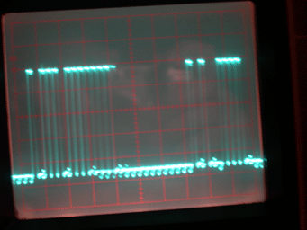 The
photo in fig. 12 has been taken on a HP-25 idling in the "wait_a_ key" loop (addr
0745, 0746), displaying “0.00”
In this architecture the 2 signals Is and Ia are mixed
on the ISA line.
The time windows are slightly different.
Each part will be details in sub chapters.
Revision 1, 7 January 2007
© Jacques Laporte 2007.
All photos J. Laporte