- Generality
- Details
- PSU
Let us start from the HP-25 basic schematic published by HP in the Nov. 1975 HP Journal edition and see  what we can discover.
1) First the machine used a 12 digit display (8 LED anodes scanned by an Anode driver, and 12 'digits' scanned by a Cathode driver, the latter being used also to scan the keyboard's 7 columns.
2) It used a new microprocessor named 'Arithmetic an Control Timing (ACT), instead of 2 chips in the Classic series.
3) It had 2 ROM chips (one being included in the Anode driver chip) and one RAM chip to store data and programs.
4) It had more (8) internal registers than the Classics.
5) It could hold 2 'return addresses' thus handling 2 subroutine calls at the microcode level.
6) Its Power Unit used 3 voltages built from the 2 NiCd (2 x 1.2V) : Vss= +6V, Vgg= -12V for the MOS chips and a new Vdisp= 4V used by the display.
Comparing this arrangement with the HP-35, 45, 55, 65, there are no TTL source clock and thus no need to transform it into a MOS clock, in a special chip.
The ACT is building itself the 2 phase clock for the PMOS chips (MOS technology requires a 2 phase clocking strategy to avoid clock skew problems).
The bus is also simplified : 4 lines : the clock's 2 phases, the Sync line and a new line names Isa multiplexing addresses and data on the system time word.
The Power on logic is also included in the ACT and only a few analog elements (4 resistors - only 2 are shown on the HP sketch, 2 capacitors, 1 inductor) are needed along with the 5 chips : ACT (PMOS), ROM1 (PMOS), RAM (PMOS) ROM0 and Anode driver (PMOS) and Cathode driver (bipolar).
The box named 'Power Supply' had a lot of analog elements, as in the older generation.
I started with these data to conduct the retro analysis of the series.
Obviously a few real machines on my bench spoke more, when 'questioned' a little bit.
Note that there is -this time- no big help like the US Patent 4,001,5692, for the HP-45 (with an object and source ROM listing, keyed in by Eric Smith in 1995).
There are 2 patents related to the HP-25, one is #3,987,290, 0ct 19, 1976, granted to Peter D. Dickinson for a "Calculator apparatus for displaying data in engineering notation", the other is #4,177,520 for a 'Calculator apparatus having a single-step key for displaying and executing program steps and displaying the result', granted to Randall B. Neff.
The latter had a partial ROM listing (4 pages and a half) but no electrical description.
The way the ACT was operating was deduced by analogy to the couple C&T + A&R and by the study of the signals coming out of it.
Two previous study were priceless. Tom NAPIER described back in 1978 the machine time word of the HP-67 (the Woodstock Masterpiece) and commented part of the ROM, and Eric SMITH wrote 'NonPareil' a ROM image emulator for the Classic and Woodstock.
The HP 25 and Woodstock instruction set is not completely new. In fact, it is an extension of the HP-35’s set. It is now completly deciphered and I wrote emulator of the HP-67 is running faithfully the ROM image code (with the operations of the card reader).
As far as the HP-21 and HP-25 are concerned I will comment in this series a portion of it (with a ROM image emulator).
All the electrical signals coming out the system show a real ressemblance with the older generation as the PMOS technology was kept.
But sometimes big differences appear driven by the fast pace of technology evolution. As a result of the integration level progress, we have here one chip for the processor and much more ROM states to store a much complex firmware.
The need for more room implied a larger address 'space'. That's why we have here 12bits instead of 10 in the Classic series and a new instruction set (an extension to be exact) to make 'programmability' easier.
The 65 and 55 were programmable and they use the instruction set of the 35.
But with the Woodstocks, HP introduced a real
computed “goto” presented as the key of a programmable calculator (partial content of register A is taken as the next microprogram address).
The Woodstock have also the instruction “delayed rom x” which was meant to ease system programmation but not obviously disassembling.
At a memory address, a Woodstock disassembler does not know statically to which rom the code belongs since a "delayed rom X" could be encountered earlier. Only a 'test run' can gather all the information.
Fortunately, I have sourced and will comment a complete assembly code with labels.
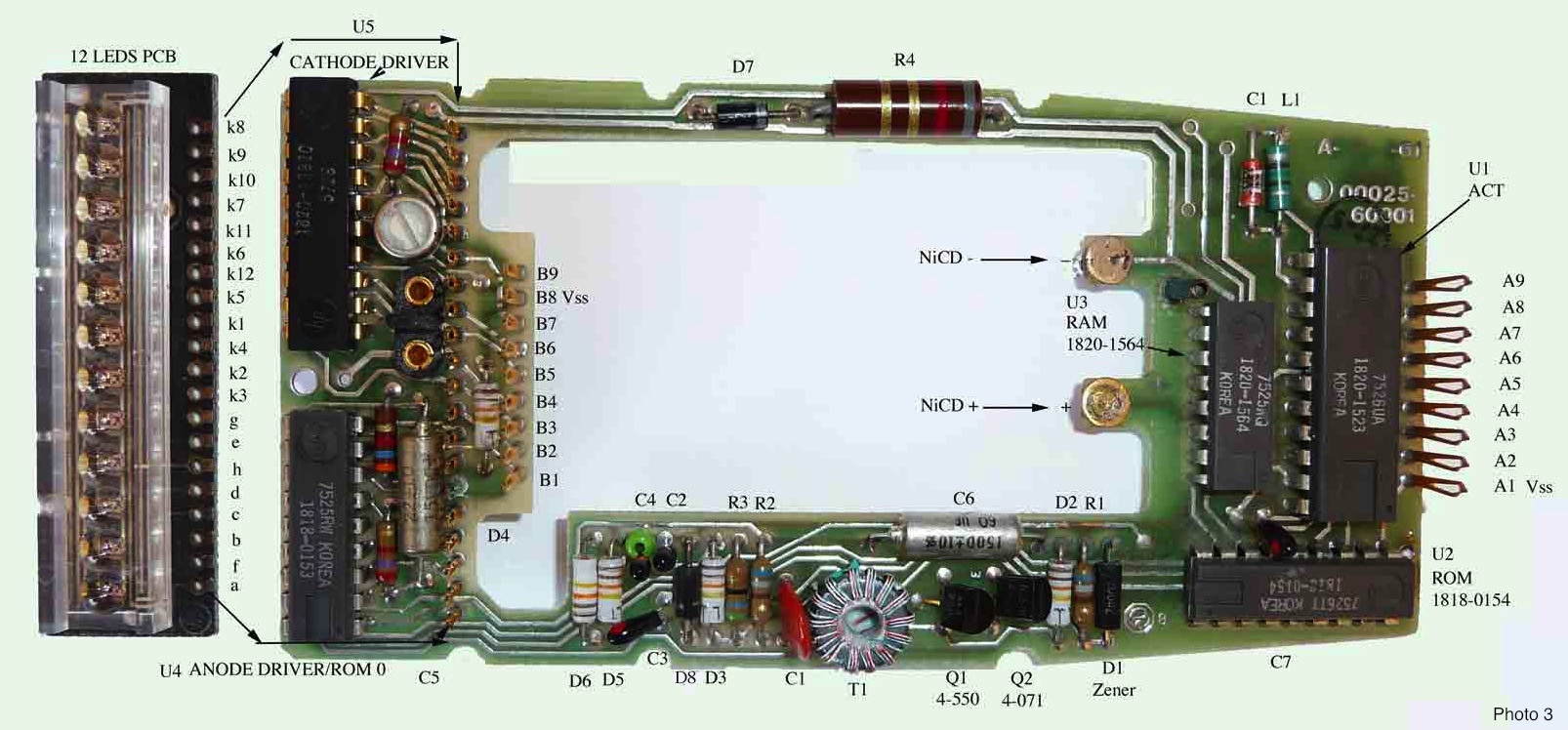
But let's start with the hardware. Here is the full schematic of a HP-25 (sorry the CAD version is late).

There are 3 chips in the HP-21 (ACT , Anode Driver + ROM, Cathode Driver) and 5 in the HP-25 (one extra ROM and the RAM chip).
The ACT is the heart of the system. It is a complete micro calculator on a chip, with a sequencer (as in the C&T circuit) and an ALU. It needs 2 voltages : Vgg (-12V) and Vss (6V).
It provides for the rest of the system the following signals,
- 2 phase clock (phi1 and phi2),
- POR (Power on Reset)
- SYNC (Address word are on ISA bus)
- ISA (Address, Data and Display bus).
The ACT's system counter is used to scan the keyboard (columns lines) ; the rows being scanned by the Cathode driver.
An important point: the bridge between the ACT (points A1-A9) side and the Cathode driver side (B2 to B9) is made by the keyboard itself (see photo 1).

From Bottom to top :
- the keyboard PCB (2 pieces heat staked),
- the LED PCB,
- the Main PCB.
Connector B = the 9 pins named B1 to B9 on the schematic :
B1 is linked with A2 (see PSU schematic),
B8 linked to A1 (Vss),
B2 to B9 are linked to the keyboard 7 rows.
Connector A = the 9 pins named A1 to A9 on the schematic :
- A1 is Vss linked to B8,
- A2 is wired to the ON/OFF switch, and if ON, A2 and A9 are linked to B1,
- A3 to A8 are linked to the keyboard 5 columns.
I have reproduced below (Fig 3) the PSU's schematic already published on this site.
Part numbers and connector pin naming are coherent with the present work (at least I tried).
Note on photo 1, the big 8.2 Ohm Carbon Composition resistor and the rectifier diode D7.
The 2 battery contacts are also visible.
When the ON/OFF switch is open (OFF), a circuit exists to charge the 2 NiCD : D7 > R4 > A2 > NiCD > Gnd.
When the machine is ON, another circuit provides current directly to the system : D7 > A9 > B1.
When the calculator is turned to the programming mode (PRGM) on the HP25 or to the DEG mode on the HP-21, Vss is brought via B1 to A3 (ACT's flag 2).
 On photo 2 the keyboard of a HP25 is shown :
-
front and back (the 2 pictures on the right),
-
and also the heat staked sandwich being separated, on the left.
On these left pictures, the keyboard PCB (front view) is very similar to that of the HP-35.
The “Cricket” keyboard with the famous "tactile feedback" is still there. A curved strip of metal is raised at key location to form a 'hump' right over a printed-circuit running underneath
Pressing the key, will depress the 'hump' and snap the metal down making contact.
The strips are spot welded to the circuit board and a matrix of traces (rows and columns) is organized.
Keyboard scanning is done by the ACT for the columns (using the system master counter) and by the Cathode Driver for the rows (while scanning a row at a time).
The “Debouncing” action is still handled by the firmware.
The 2 calculators used only 3 voltages:
- Vss @ 6V DC,
- Vgg @ -12V DC and
- Vdisp @ 4V DC for the display circuits.

The DCDC converter has already been discussed on this site. It is a simple blocking oscillator based on 2 NPN transistors:
- one Q2 on the schematic is forming the blocking oscillator (winding B and A and capacitor C1),
- the other Q3 being with the Zener diode D1 the regulator circuit.
This part is rather standard in HP calculators.
The battery charger is more rock and roll.
A simple transformer (10 V AC) is providing current to a diode D7 and a resistor R4 which is connected to the positive pole of the 2 NiCD battery cell.
The charging current is around 125 mA., from point A2 to gound through the NiCD.
Note that the batteries are forming a clamping circuit, keeping A2 @2.5 DC.
If HP project leaders asked for a cheap charger, they sure got it with this one!
It worked and sometimes still works, but prey for a good contacts at battery connectors, which happen to be the weakest part of the machine's PSU when age comes with corrosion etc ....
If the circuit through the NiCd is open, the clamping effect no longer exist
bringing point A2 to a higher -and possibly fatal- potential.
The PCB layout around the 2 NiCd batteries can be divided in 4 parts (see photo 3) :
- the ACT side with the ACT (U1), the ROM (U2), and the RAM (U3) chip,
- the display side (left), with the Cathode (U5) and Anode Drivers with ROM (U4) and the 12 LED PCB that plugs in the 12 pins connector,
-
the PSU side (bottom) the DC-DC converter (17 discrete components),
-
and top the rectifier diode D7 and the 2W, 8.2 Ohm R4 resistor that form together the current source to charge the batteries (the 10V AC connector is the 2 golden ring plug near the cathode driver). Note that the protective diode D8 is mounted only in the HP-25.
Now, the whole story in details.
Now some hardware details.
Here is the Woodstock timing (HP21, 25 ... and HP-67, 97).

The system clock runs at 180khz that is to say 5.5 μseconds for each period.
Each clock pulse is about 0.7 us.
The clock is distributed in the system with a 2 phase strategy, to avoid clock skew in the PMOS latches.
The whole word time is 56 pulses long ; just like the Classics. That's about 310 micro seconds.
It is the time it takes to a 14 dig it register to circulate on the serial bus (to or from memory) : 14 * 4 = 56.
A LC cell is tuning the frequency : 330 pf and 150 uH ; that is 715Khz 1/(2 * pi * SQRT(LC)) divided 2 times by 2 gives 180 Khz.
The signal SYNC (photo 1 - 10 pulses can be seen) is high during the 'instruction' time (10 bits).
All data on the bus use the same serial line ISA (on the Classics, 2 lines were used).
Note another time window (8 bit long) from bit0 to bit7, used by the ACT to send data to the display system (anode + cathode driver), digits and flags, one digit every 56 period cycle.
The 2 phase clock (photo 2) is derived from an oscillator whose wave are shown on photo 3 (ACT's pin 13). This MOS clock (swing +6/-12) is distributed to the PMOS chips (on the 25, RAM chip, ROM chip and Anode driver chip).
The Cathode driver is still bipolar.
The ISA (photo 4) and SYNC signals goes to the same chips.
A counter (probably the sequencer's master counter) is used in the ACT to scan the keyboard's 5 columns, pins A4, A5, A6, A7, A8 of the A connector (ACT side).
The cathode driver does the same for the 7 rows, pins B5, B3, B2, B4, B6, B9 of the B connector opposite side.
The ACT is also sensing line A3 which is connected internally to the RUN/PRGM on the 25 and DEG/GRAD on the 21 (Vbatt on A3 is PRGM etc..).
An important point is that the HP-35 inductive display
is gone.
The Anode Driver chip is sourcing enough current to handle the 8 anodes of each LED digit.
An extra 4V DC voltage is needed (Vdisp on my schematic).

The HP-21 & HP-25 has one ROM (ROM0) included in the Anode driver chip.
The 25 has a extra chip for extra firmware.
Let's compare :
- on the HP-35 there was 3 ROM chip fora total of 768 instructions (10 bit instructions, 8 bit addresses),
- on the HP-21 we find 1 ROM chip, for a total of 1024 instructions (10 bit instructions, 12 bit addresses),
- on the HP-25 we have 2 ROM chips, for a total of 2048 instructions (10 bit instructions, 12 bit addresses).
The 21 had 30% more ROM space than the HP-35, to store the same functions plus the versatile display formatting,
radian mode trigo, polar to rectangular conversion and storage arithmetic STO + X etc..
But the display was shorter : 12 digits instead of 15, to fit in the new plastic case (narrow, cheap but robust).
Both calculators (21 and 25) still had 10-digit precision. The display was reengineered consequently.
The decimal point was moved next to a digit and two of the display digits play a double role, mantissa and -when needed- exponent sign and digit.
The HP-25 has a RAM chip with a serial input (pin 4 linked to pin 10 of the ACT).
Note they are few passiv e components :the LC cell, the Power on Reset capacitor, the display current resistor and the battery sensing 2 resistors + 1 pot.
A link between the Anode driver (pin 11) and the Cathode driver (pin 14) has the obvious function : stepping digits.
The RCD line is resetting the cathode driver from the ACT.
The new microprocessor ACT (Arithmetic, Control & Timing circuit) uses 12 bit addresses and one ROM
(2 in the HP-25 but more in the HP-67 for example), is selected only when relevant address is place on the ISA line,
no more enable flip/flop mechanism.
Subroutine calls can be located on different ROMs and return addresses (12 bits) will get back to the correct place.
No more code relay between ROMs.
Two levels of stack are available : a subroutine can call another one..
Two other type of instructions give more power to microprogrammer:
- data register accessing instructions ( "c -> data address", "c -> data", "data -> c" etc...),
- and register to ROM addressing ("a -> rom address").
The later instruction takes 2 calculated digits as the next micro program counter (like a computed GOTO instruction).
According to HP it "made the HP-25 possible.
Let us take an example (see the HP-25 ROM listing commented in the firmware pages).
When decoded the
key phrase 'STO 2' (key code 2a) branches to 017771 octal where the control finds a '0010010000'
op code : the "a -> rom address" instruction.
Register A = 2100000000012a" ; the target address is computed with PC=1771o, a[2] and a[1] : 17771o AND (NOT 0377o) = 1400o that is to say 0300h + 10h (a[2] << 4) + 2 (a[1]) = 312h =1422octal, and so on.
Now, let's see how the new microprocessor compares with the C&T+A&R couple in the Classic.
It is not easy to benchmark the micro coded operations, but it's possible to measure operations in a 60 second loop for programmable calculators.
I took a HP-55 (C&T+A&R as in all Classics) and a HP-25 (both programmable) :
HP-25 :
RCL 0
ln x
1
STO + 0
GTO 0,
HP-55 :
RCL
0
f
ln
1
STO
+
0
GTO 01
The HP-25 made 210 ln X operations, in one minute, while the HP-55 only 180.
Faster but not very much.

HP-25 Instruction Set
The ACT's internal organization and the instruction set are evolutions of the previous ones.
We find registers A, B, C, Y, Z and T like in the HP-35.
The scratchpad memory is doubled M1 and M2.
And a nibble register 'F' is now making easier the digit count when entering a number.

- A, B: are general purpose registers,
- C: holds the normalized form, A has the displayable floating point form,B holds a mask to position the decimal point (after ‘$outputz’ and ‘rounda’ cf. firmware comments),
- D, E, F: operational stack levels Y, Z, and T,
- M1: scratchpad register (transfers to and from the C register),
- M2: scratchpad register (transfers to and from the C register),
- P: 4 bit "pointer" register used for register field addressing (offset into the registers -> 14),
- F: is a ‘nibble’ register holding part of a[0],
- s[0]-s[15]: The status register is now equipped with a 16 bits of status (one position s[15] being used by the hardware).
Just like on the Classics, operations with a field select option allow part of each 56 bit register to be accessed
('000' to '111' see the arithmetic instruction below).
| m | mantissa |
| ms | mantissa and sign |
| x | exponent |
| xs | exponent and sign |
| s | mantissa sign |
| p | pointer |
| w | word (14 digits) |
| wp | word up to the nibble pointed by the p register |
Also, the masking logic has been completely changed to handle the new display and the new notation scheme (SCI and ENG).
Note that M1, M2, and F are memory registers internal to the ACT.
External RAM memory is organized in 'registers' of 14 digits (56 bits):
- 8 data storage registers (R0 .. R7),
- one Last x register,
- 7 user program registers (one byte per step ; 7 steps per register ; 7 * 7 = 49 steps).
Instructions are coded as a 10 bit word.
There are 4 types of instructions, named after their 2 rightmost bits.
'01' type : [a,a,a,a,a,a,a,a,0,1]'jsb' - it is the subroutine call,
'11' type :
[a,a,a,a,a,a,a,a,1,1]'goto' - it is the n/c go to 'addr' instruction (addr is an 8 bit address 0-255)
'10' type :
[x,x,x,x,x,w,w,w,1,0]it is the 'arithmetic' instruction group ; there are <xxxxx> 32 possible operations on <www> 8 'fields'.
<xxxxx> 32 operations
0: 0 -> a
1: 0 ->b
2: a <->b
3: a ->b
4: a <->c
5: c ->a
6: b ->c
7: b <->c
8: 0 ->c
9: a + b ->a
10: a + c >a
11: c +c ->c
12: a +c ->c
13: a +1 ->a
14: SL a[ ]
15: c +1 ->c
16: a -b ->a
17: a -c ->c
18: a -1 ->a
19: c -1 ->c
20: 0 -c ->c
21: 0 -c-1 ->c
22: if b[ ] = 0
23: if c[ ] = 0
24: if a>= c[ ]
25: if a>= b[ ]
26: if a[ ] # 0
27: if c[ ] # 0
28: a - c -> a[ ]
29: SR a[ ]
30: SR b[ ]
31: SR c[ ]
Operating on 8 fields
000: p
001: wp
010: xs
011: x
100: s
101: m
110: w
111: ms
e.g: addr 343, addr 1110111010, shift right a[w ], ==>> type ='10', operation= 11101 (29dec) : SR a[ ], field = 110 : 'w' (whole word).
'00' type :
[x,x,x,x,y,y,y,y,0,0]it is a miscellaneous type, where yyyy is a subtype code (16 subtypes) possibly taking <xxxx> 16 'arguments' each.
[0,0,0,0,0,0,0,0,0,0]: no op (eg: addr=2541o),
[x,x,x,x,0,0,0,1,0,0]: 1 -> s[ ] (eg: addr=0633o = [1,0,0,1,0,0,0,1,0,0]= 1 -> s[9 ], '1001'=9dec, (1)
[x,x,x,x,0,0,1,0,0,0]: this subtype is a class '0010' that has 16 different meanings depending on its argument:
[0,0,0,0,0,0,1,0,0,0]= clear registers (eg: addr 2317o),
[0,0,0,1,0,0,1,0,0,0]= clear status (eg: addr 2245o),
[0,0,1,0,0,0,1,0,0,0]= display toggle (eg: addr 0276o),
[0,0,1,1,0,0,1,0,0,0]= display off (eg: addr 0762o),
[0,1,0,0,0,0,1,0,0,0]= m1 < - > c(eg: addr 0244o),
[0,1,0,1,0,0,1,0,0,0]= m1 - > c(eg: addr 0255o),
[0,1,1,0,0,0,1,0,0,0]= m2 < - > c(eg: addr 0246o),
[0,1,1,1,0,0,1,0,0,0]= m2 - > c(eg: addr 0305o),
[1,0,0,0,0,0,1,0,0,0]= stack - > c (eg: addr 02171o),
[1,0,0,1,0,0,1,0,0,0]= down rotate (eg: addr 01245o),
[1,0,1,0,0,0,1,0,0,0]= y - > a (eg: addr 02133o),
[1,0,1,1,0,0,1,0,0,0]= c - > stack (eg: addr 02035o),
[1,1,0,0,0,0,1,0,0,0]= decimal (eg: addr 0056o),
[1,1,0,1,0,0,1,0,0,0]= unassigned,
[1,1,1,0,0,0,1,0,0,0]= f - > a (eg: addr 0135o),
[1,1,1,1,0,0,1,0,0,0]= f < - > a (eg: addr 0173o),
[x,x,x,x,0,0,1,1,0,0]: 0 -> s[ ] (eg: addr=0315o = [1,1,1,1,0,0,1,1,0,0]= 0 -> s[15 ], '1111'=15dec, (2)
[x,x,x,x,0,1,0,0,0,0]: this subtype is a class '0100' that has 9 different meanings depending on its argument:
[0,0,0,0,0,1,0,0,0,0]= keys -> rom address : (eg: 0770o only occurrence in Rom), branches to Rom addr according to key code,
[0,0,0,1,0,1,0,0,0,0]= not used in HP-25 (HP-67 inst. set),
[0,0,1,0,0,1,0,0,0,0]= a -> rom address : compute address based on A register and go to this address in Rom (eg: 01771, address in a[2] and a[1]),
[0,0,1,1,0,1,0,0,0,0]= not used in HP-25 (HP-67 inst. set),
[0,1,0,0,0,1,0,0,0,0]= binary (eg: 0763o), set arithmetic unit to binary mode,
[0,1,0,1,0,1,0,0,0,0]= not used in HP-25 (HP-67 inst. set),
[0,1,1,1,0,1,0,0,0,0]= p - 1 -> p (eg: 0472o)
[1,0,0,0,0,1,0,0,0,0]= p + 1 -> p (eg: 0045o)
[1,0,0,0,0,1,0,0,0,0]= return (eg: 0170o)
[x,x,x,x,0,1,0,1,0,0]: if s[7]=1 where 'xxxx' is the flag number (eg: addr=0035o = [0,1,1,1,0,1,0,1,0,0]= if s[15 ] =1 , '0111'=7dec) : test if status flag 7 is set,
[x,x,x,x,0,1,1,0,0,0]: load constant 'xxxx', (eg: 0405o) : load constant 12 (hex 0c) in the byte pointed by pointer p,
[x,x,x,x,0,1,1,1,0,0]: if s[3]=0 where 'xxxx' is the flag number (eg: addr=0072o = [0,0,1,1,0,1,1,1,0,0]= if s[3 ] reset, '0011'=3dec) : test if status flag 3 is reset,
[x,x,x,x,1,0,0,0,0,0]: select ROM 'xxxx' (eg: 0467, select rom 3, '0011100000' (0011=3dec) where 'xxxx' is the selected rom space (3),
[x,x,x,x,1,0,0,1,0,0]: if p = 'xxxx' (eg: 01510o if p = 13 '1101100100' (1101=13dec), test if point p has the specified value,(arg)= 'xxxx' is indexing { 4, 8, 12, 2, 9, 1, 6, 3, 1, 13, 5, 0, 11, 10, 7, 4 }
[x,x,x,x,1,0,1,0,0,0]: c -> data register 'xxxx' (eg: 02357, '0000101000' store dat in c to register 0) ; 'xxxx'= 0 to 7
[x,x,x,x,1,0,1,1,0,0]: if p # 'xxxx' (eg: 02744o if p # 12 '0010-101100' (0010=2dec) (arg)='xxxx' is indexing { 4, 8, 12, 2, 9, 1, 6, 3, 1, 13, 5, 0, 11, 10, 7, 4 })
[x,x,x,x,1,1,0,0,0,0]: this subtype is a class '1100' that has 6 different meanings depending on its argument:
[0,0,0,0,1,1,0,0,0,0]= not used in HP-25 (HP-67 inst. set),
[1,0,0,1,1,1,0,0,0,0]= c -> data address, (eg: 1550, in 'fetch' routine) : points data base address in Ram ; address is in c[1] and c[0],
[1,0,1,0,1,1,0,0,0,0]= clear data regs, ( eg: 0237), clears all data ram registers (16 reg : 8 data storages, 1 last_x, 7 PRGM storages).
[1,0,1,1,1,1,0,0,0,0]= c -> data (eg: 1543 in routine 'thru1', update register pointed by 'data address')
[1,1,0,0,1,1,0,0,0,0]= not used in HP-25 (SPICE inst. set),
[1,1,1,1,1,1,0,0,0,0]= 'hi i'm woodstock' one occurrence in ROM 00753o : No Op,
[x,x,x,x,1,1,0,1,0,0]: delayed rom 'xxxx' (eg: 02122o 0111 110100 delayed rom 7 ; 0111=7 ), Rom change is delayed until the next branch instruction,
[x,x,x,x,1,1,1,0,0,0]: data register 'xxxx' -> c or shorter data -> c (eg: 02230o : '0011 111000' register 3-> c ; 0011=3),
[x,x,x,x,1,1,1,1,0,0]: p < - x ; set p to the value x ; (eg: 00041o 1000 111100 p <- 1 '1000'= 8 is an index in { 14, 4, 7, 8, 11, 2, 10, 12, 1, 3, 13, 6, 0, 9, 5, 14 },
(1) note the assembler form '1 -> s f 9' where 9 is the index and 'f' is a mnemonic : this flag is set when the prefix 'f' (yellow) is pushed),
(2) note the assembler form '0 -> s key 15' where 15 is the index and 'key' is a mnemonic : in the $wait loop, the flag 15 is reset (no key pressed),
(3) 'xxxx' is a 256 bytes ROM space and not a physical chip.
Jul 03, 2011
The schematic (already given) is there as reminder.
The ON/OFF switch on the schematic shows that when ON the calculator's circuits are fed directly while the batteries are charged.
Clearly the designer wanted to kill two birds with one stone : charging the battery with a constant current and feeding the calculator with a regulated voltage.
The voltage source is a transformer and a single diode.
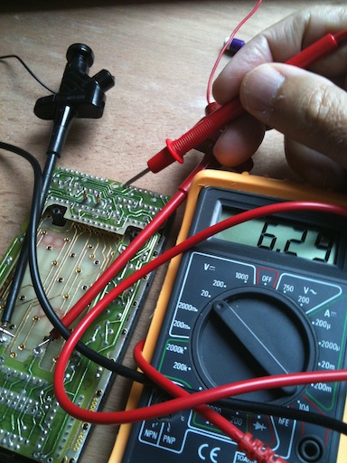
The passive current source is the voltage source plus a simple resistor providing a charging current of around 125 mA, from point A2 to ground through the 2 NiCds.
The 2 NiCds have a clamping effect : the voltage at A2 is around 3V (around 3-3.3V OFF and 2.75-2.95 ON).
This is a flaw in the conception, to say the least.
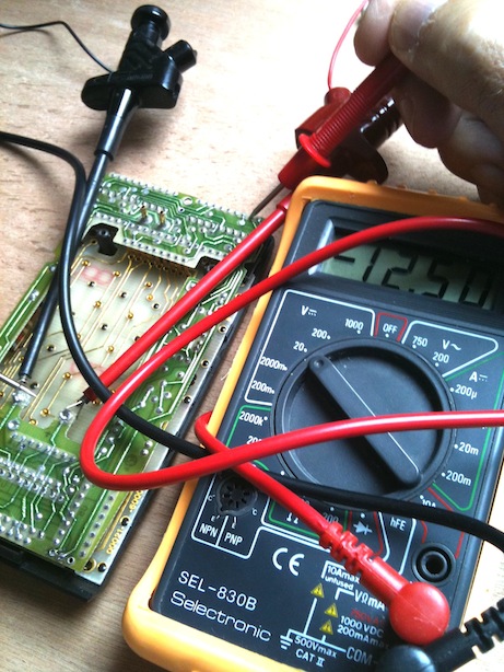
When the 2 NiCads are removed (or have bad contacts), the clamping effect doesn't exist anymore, and the voltage at point A2 is too high (>> 5V) and possibly lethal for the MOS circuits.
See below my video showing the experiment.
The so-called adapter is in fact a simple transformer on a PCB.
 Photo 1 - Adapter charger
HP 82026A 115 V / 230 V (switchable) - USA
Here is the schematic of the charging circuit for Woodstock calculators.
HP 82024A 115 V / 230 V - EU
HP 82025A 220 V - EU
HP 82026A 115 V / 230 V - USA
HP 82041A 220 V - EU
HP 82041C 110 V - USA
For more details on HP adapters, please see the Kees Van der Sanden's web site:

When the charging circuit is closed (switch = ON) the 2 batteries are charged through the 8.2 resistor and the calculator is fed directly. Clearly, on the scope (see below photos and video) the Nicad pack is droping down the Vbatt voltage to 3Vdc.
The experiment -on the video below- is showing the effect of a missing battery pack on the HP-25 power supply unit.
On old machines corrosion often cuts the electrical continuity between the charging circuit and the 2 Nicads.
The footage shows clearly the possibly damaging voltage rise.
e's probe has been plugged at the entry of the PSU circuit, on D7's Anode.
(photo 3, below).
Photo 4 shows the signal at point A2 : the NiCads' clamping effect is shown but the voltage is not yet filtered.
On the last 3 photos, the 3 voltages are probed, according the schematic.

Photo 3
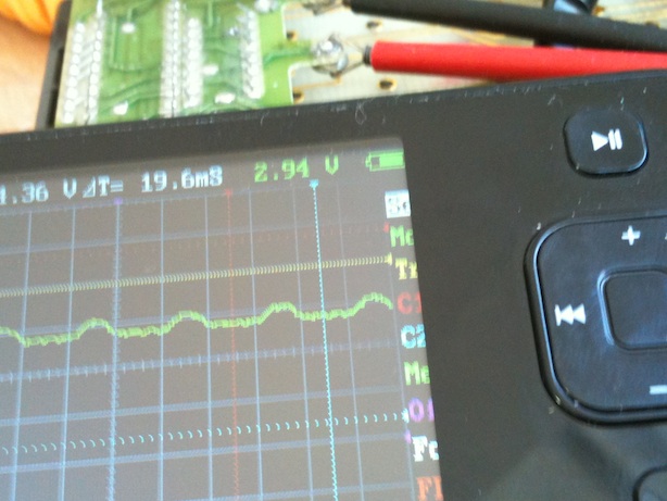
Photo 4

Now the schematic in Cadence and the associated simulation in Pspice.
The 3 DC voltages (6V, 4V and -12V) generated by the PSU are simulated and the 'display' Vdisp (4V DC) is well 'predicted' by Pspice.
The 2 NPN as taken as 2N3704.


June 23, 2011